
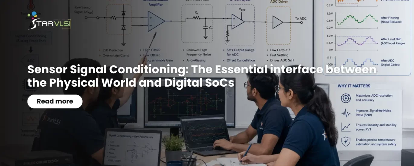
Sensor Signal Conditioning: The Essential Interface Between the Physical World and Digital SoCs
SoCs operate in the digital domain, but the real world speaks in small, noisy, nonlinear analog signals. Signal conditioning is the chain of analog and mixed-signal techniques — amplification, filtering, level shifting, linearization, and calibration — that turns a raw sensor output into something an ADC can digitize accurately. Using a temperature sensor as a running example, this article walks through why a sensor can't connect directly to an ADC, what a full conditioning chain looks like, and why analog front-end quality ultimately limits system accuracy, no matter how good the ADC is.
Sensor Signal Is Not Connected Directly to the ADC
Modern System-on-Chip (SoC) designs are increasingly becoming the intelligence hub of automotive, industrial, medical, consumer, and IoT systems. However, most of the SoC operates fundamentally in the digital domain, while most real-world information originates as physical phenomena such as temperature, pressure, acceleration, light, gas concentration, humidity, or vibration.
This creates a fundamental interface problem: how does a digital SoC accurately understand a small, noisy, and often nonlinear electrical signal generated by a sensor? The answer is sensor signal conditioning — the collection of analog and mixed-signal techniques used to transform the electrical output of a sensor into a clean, stable, and appropriately scaled signal that can be digitized and processed reliably by the digital portion of the SoC.
A typical sensor-enabled SoC therefore looks conceptually like this:
The quality of digital information is therefore strongly dependent on the signal before the ADC.
A common assumption in SoC design is that the ADC can simply sample whatever voltage comes from the sensor. In practice, this approach can produce poor accuracy or even completely unusable measurements.
A sensor output may have a very small amplitude. A temperature sensor, for example, may produce only a few millivolts per degree or may exhibit a resistance change rather than a directly measurable voltage. A pressure sensor may produce a differential output of only a few millivolts over its operating pressure range.
The sensor signal can also contain electrical noise, interference from switching circuits, power-supply disturbances, and electromagnetic coupling. Sensor characteristics may vary with temperature, process, supply voltage, and manufacturing tolerances.
The ADC has requirements regarding input range, source impedance, sampling rate, and settling time. Therefore, the signal-conditioning circuitry must transform the raw sensor output into a signal that makes maximum use of the ADC's dynamic range while maintaining the required accuracy.
The Signal-Conditioning Chain
Signal conditioning is not one particular circuit — it is a combination of functions selected according to the sensor technology and system requirements. A typical signal-conditioning chain may contain sensor excitation or biasing, buffering, amplification, filtering, level shifting, linearization, offset cancellation, protection, and finally an ADC interface.
The objective is to convert a weak, noisy, and possibly nonlinear sensor signal into a clean, accurate, and ADC-compatible signal. For a sensor producing a differential output, the chain may look like:
Low-Level Signal
Not every application requires every block. The architecture depends on sensor type, signal amplitude, bandwidth, accuracy, environmental conditions, and SoC technology.
Temperature Sensor as a Signal-Conditioning Example
Temperature sensing provides a particularly useful example because several different sensing technologies are available. A temperature sensor may generate a voltage proportional to absolute temperature, a voltage proportional to temperature difference, a resistance variation, or a current proportional to temperature.
In an SoC, a commonly used integrated temperature-sensing approach is based on semiconductor junction characteristics. The forward voltage of a bipolar junction device has a temperature dependency, while the difference between the base-emitter voltages of devices operating at different current densities produces a quantity approximately proportional to absolute temperature. This is commonly referred to as a ΔVBE-based temperature-sensing principle.
The sensor output is normally not sent directly into digital logic — it must first be converted into a well-defined electrical quantity.
Bringing the Output into the ADC Range
One of the most important signal-conditioning operations is amplification. Suppose a temperature sensor generates a signal ranging from 200 mV to 300 mV, while the ADC has a 0–1.2 V input range. Directly connecting the sensor to the ADC uses only a small portion of the available ADC range.
An amplifier is used to bring the sensor output to the ADC range — i.e., to amplify the 200 mV–300 mV signal to a peak-to-peak voltage of 1.2 V. The gain must be selected carefully so that the maximum expected sensor output does not exceed the ADC input range.
In precision temperature sensing, offset and gain errors of the amplifier can become significant because the temperature signal may be relatively small. Low-offset amplifiers, chopper-stabilized amplifiers, auto-zero techniques, or digitally calibrated architectures may therefore be considered.
Filtering: Removing Noise Before Digitization
Sensors are frequently located close to motors, switching regulators, RF circuits, clocks, and high-speed digital interfaces. Consequently, the sensor output may contain noise that has nothing to do with the physical parameter being measured.
An RC low-pass filter with a proper cutoff frequency is commonly used when temperature changes relatively slowly. Temperature normally changes much more slowly than high-frequency electrical noise, so a low-pass filter can significantly improve the signal-to-noise ratio before conversion. The design must, however, consider the ADC sampling frequency and settling time — an excessively aggressive filter may introduce unwanted delay or prevent the ADC input from settling correctly.
Offset Removal and Level Shifting
The sensor output may contain a large DC offset in addition to the temperature-dependent signal. If the useful temperature information is represented by only a small change around a large offset, an ADC can waste a significant portion of its dynamic range.
An analog conditioning stage can subtract the known offset and amplify the remaining signal. Offset correction can also be implemented digitally, but removing large unwanted components before the ADC can improve the effective use of ADC resolution.
Linearization of Temperature Sensors
Real sensors are not always perfectly linear. Linearization can be performed in the analog domain, digital domain, or through a combination of both. Modern SoCs often prefer digital correction because it provides flexibility — the ADC digitizes the sensor output, and calibration coefficients or lookup tables are then used by digital logic to calculate the corrected temperature.
A Practical Temperature-Sensor Signal-Conditioning Circuit
A simplified integrated temperature-sensor interface can therefore contain the following blocks:
| # | Block | Function |
|---|---|---|
| 1 | BJT / Diode Sensor | Generates the ΔVBE-based temperature-dependent signal |
| 2 | Differential Instrument Amplifier | Rejects common-mode noise, extracts the differential signal |
| 3 | Amplifier | Scales the signal to use the full ADC dynamic range |
| 4 | RC Active Filter | Removes high-frequency noise and prevents aliasing |
| 5 | ADC | Digitizes the conditioned analog signal |
| 6 | Digital Filter | Further smooths the digitized data stream |
| 7 | Calibrator | Compensates for process, voltage, and temperature variation |
| 8 | Linearization | Corrects nonlinearity using coefficients or lookup tables |
This architecture is particularly relevant when temperature sensing is integrated directly into an SoC for monitoring the CPU, GPU, analog blocks, power-management circuits, or other heat-generating regions.
Sampling and Anti-Aliasing Are Critical
Signal conditioning must also consider the ADC sampling process. If a high-frequency noise component exists above half the ADC sampling frequency, it can alias into the sampled signal and appear as a false low-frequency component.
The basic Nyquist relationship is: fs > 2fmax, where fs is the sampling frequency and fmax is the highest signal frequency of interest.
In practice, an anti-aliasing low-pass filter is placed before the ADC. For a slowly varying temperature signal, the required bandwidth may be very low, allowing substantial filtering of unwanted high-frequency noise.
Digital Signal Conditioning After the ADC
Signal conditioning does not necessarily stop at the ADC. Once the sensor signal has been digitized, additional processing such as digital low-pass filtering, offset correction, gain correction, and linearization may be needed in digital logic. Digital filtering can use moving-average filters, IIR filters, FIR filters, or application-specific filtering algorithms. Digital calibration coefficients can also compensate for manufacturing variation in the sensor and analog front end.
Calibration Needs
Even carefully designed sensor circuits exhibit variations because of semiconductor process, voltage, and temperature effects. For an integrated temperature sensor, two chips manufactured using the same process may produce slightly different raw sensor outputs at the same physical temperature. Calibration can compensate for this variation.
Sensor Interface Design Is a Mixed-Signal SoC Problem
The sensor signal-conditioning interface includes the sensor, analog front end, ADC, reference, clocking, digital processing, calibration memory, and software interface. Power supply isolation, analog and digital ground strategy, clock noise, substrate coupling, layout, shielding, and placement of the sensor interface can all influence the final measurement accuracy.
From Temperature to Other Sensors
The same signal-conditioning philosophy applies to many other sensors. Although the sensor technologies differ, the fundamental signal chain remains similar: Sense → Condition → Filter → Convert → Calibrate → Process.
Designing the Signal-Conditioning Circuit for an SoC
When integrating sensor conditioning into an SoC, the designer needs to start from sensor characteristics rather than with the ADC alone. The sensor's output range, sensitivity, source impedance, bandwidth, noise characteristics, and temperature dependence determine the required analog front end.
The ADC resolution, reference voltage, sampling rate, and input requirements then determine how the conditioned signal should be presented to the converter. Finally, digital architecture must provide the required filtering, calibration, linearization, and system-level processing.
A well-designed sensor interface therefore involves close cooperation between analog designers, mixed-signal designers, RTL designers, verification engineers, physical designers, and embedded software developers.
Verification of Sensor Signal Conditioning
Verification should cover both analog behavior and digital interpretation. At the analog level, designers need to verify gain, offset, bandwidth, noise, linearity, common-mode range, settling time, and PVT variations. At the ADC and digital boundary, the design needs to be checked for quantization behavior, sampling errors, overflow, saturation, and calibration accuracy.
A mixed-signal verification environment can inject realistic sensor waveforms into the analog front end and verify the final digital temperature result.
The Bigger Picture: Sensor Interfaces Are Becoming SoC Building Blocks
As intelligent systems increasingly interact with the physical world, sensor interfaces are becoming fundamental SoC components rather than external peripherals. An automotive SoC may monitor temperature, pressure, gas concentration, battery parameters, and mechanical conditions. An industrial SoC may combine vibration, pressure, and temperature sensing. An IoT SoC may integrate environmental sensors with wireless connectivity and ultra-low-power processing.
In all these applications, the quality of the final digital decision depends on the quality of the analog signal presented to the ADC. The boundary between sensing and computing is therefore no longer simply a sensor-to-processor connection — it is an integrated sensor-to-analog-front-end-to-ADC-to-digital-processing architecture.
Conclusion
Sensor signal conditioning is the critical bridge between the physical world and digital intelligence. A sensor rarely produces an ideal signal that can be directly consumed by an SoC — its output may be weak, noisy, nonlinear, offset from the desired operating range, or sensitive to process and environmental variations.
Amplification, buffering, filtering, level shifting, offset correction, linearization, and calibration transform that raw signal into a form an ADC can digitize accurately. The temperature-sensor example demonstrates the complete concept: the physical temperature is converted into a sensor-dependent electrical quantity, conditioned through an analog front end, filtered and digitized, and finally corrected through digital processing.
For SoC designers, the key lesson is straightforward: a high-performance digital processor cannot compensate for a poorly conditioned sensor signal. The quality of sensing begins in the analog front end and ends with intelligent digital processing. Successful sensor-enabled SoCs therefore require carefully co-designed analog, mixed-signal, and digital architecture.
Master Mixed-Signal SoC Design with StarVLSI
StarVLSI brings these concepts closer to practical VLSI engineering by connecting semiconductor fundamentals with real-world SoC design methodologies.
Explore StarVLSI CoursesStay connected with the StarVLSI Blog for more in-depth articles on advanced VLSI design, sensor designs, and emerging technologies shaping the future of the semiconductor industry.