
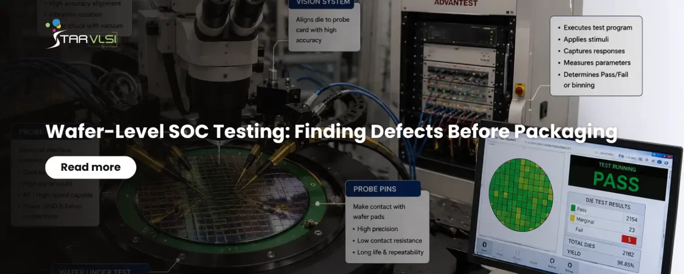
Wafer-Level SoC Testing: Finding Defects Before Packaging
Testing an SoC doesn't start after packaging — it starts on the wafer itself. Wafer-level testing (WLT) lets automated test equipment probe every die while it's still part of the silicon wafer, catching defective dies before they reach expensive packaging and final-test stages. This article covers what wafer-level testing checks, the full test flow from fab to package, the physical test setup (prober, probe card, probe pins, ATE), and why wafer maps have become a key feedback loop between SoC design, manufacturing, and yield engineering.
What Is Wafer-Level Testing?
In modern SoC development, testing starts before the chip is packaged. Wafer-level testing (WLT) provides an important opportunity to verify the functionality and manufacturing quality of individual dies while they are still part of the silicon wafer. This ensures that no failed die undergoes packaging.
After wafer fabrication, the wafer contains hundreds or thousands of identical SoC dies. Before the wafer is diced and individual dies are packaged, automated test equipment (ATE) uses probe cards to make electrical contact with each die. This process is commonly known as wafer sort or wafer probe testing. The objective is to identify defective dies early and prevent them from proceeding to the expensive packaging and final-test stages.
What Wafer-Level Testing Checks
Wafer-level testing typically checks critical electrical and functional characteristics of the SoC. Depending on the device, this can include power-supply current, leakage, clock operation, memory functionality, processor operation, high-speed interfaces, analog blocks, and selected RF or mixed-signal functions.
For complex SoCs, Design-for-Test (DFT) structures such as scan chains, MBIST, boundary scan, test controllers and built-in self-test circuits are essential. These structures allow the tester to access and diagnose internal circuitry that cannot be directly observed through external pins.
The Test Flow
The typical wafer-level test flow moves from silicon straight through to package test:
During probing, automated equipment contacts each die according to a predefined test program. The results are recorded against the physical location of the die on the wafer, creating a wafer map that identifies good, marginal, and failed dies.
Importance of Wafer-Level Testing for SoC Design
WLT has a direct influence on SoC architecture and DFT planning. Test access, scan compression, memory BIST, power-domain control, clock-test modes and analog test structures must all be considered during the design stage.
It also helps semiconductor manufacturers identify systematic manufacturing problems. If failures are concentrated in a particular region of the wafer or associated with a specific electrical parameter, the data can provide valuable feedback to the process and yield teams.
The Wafer-Level Test Setup
A typical wafer-level test setup consists of four major elements:
Probe-card design becomes increasingly challenging as pad count increases and pad pitch decreases.
Probe Card Development Is Part of the Test Strategy
Probe-card development cannot be treated simply as an external manufacturing activity. It should be considered during SoC test planning, because the number and arrangement of test pads, power domains, ground requirements, and high-speed signals directly influence the probe interface.
For advanced SoCs, the test architecture may include dedicated test pads, scan access, JTAG, MBIST, analog test points, and high-speed test structures. A well-planned interface can significantly reduce wafer-test complexity and improve test coverage.
From Test Results to Wafer Maps
Each die receives a test result, commonly resulting in pass/fail or multiple quality bins. These results are mapped back to the physical wafer location to generate a wafer map.
The wafer map is more than a production record. Spatial patterns of failures can reveal process-related problems, contamination, lithography issues, power-distribution problems, or other systematic defects — making wafer testing an important feedback mechanism between SoC design, semiconductor manufacturing, and yield engineering.
Conclusion
Wafer-level testing is a critical bridge between SoC design, silicon manufacturing, and production quality. Effective DFT architecture makes complex SoCs testable, while wafer-test data provides valuable insight into silicon quality and manufacturing yield. For advanced SoCs, designing with wafer-level test requirements in mind from the beginning can significantly reduce production risk and improve overall test efficiency.
Master DFT and Test Engineering with StarVLSI
Build hands-on expertise in DFT architecture, wafer-level test planning, and yield analysis to prepare for modern SoC test and manufacturing roles.
Explore StarVLSI CoursesStay connected with the StarVLSI Blog for more in-depth articles on current and future trends shaping the semiconductor industry.