
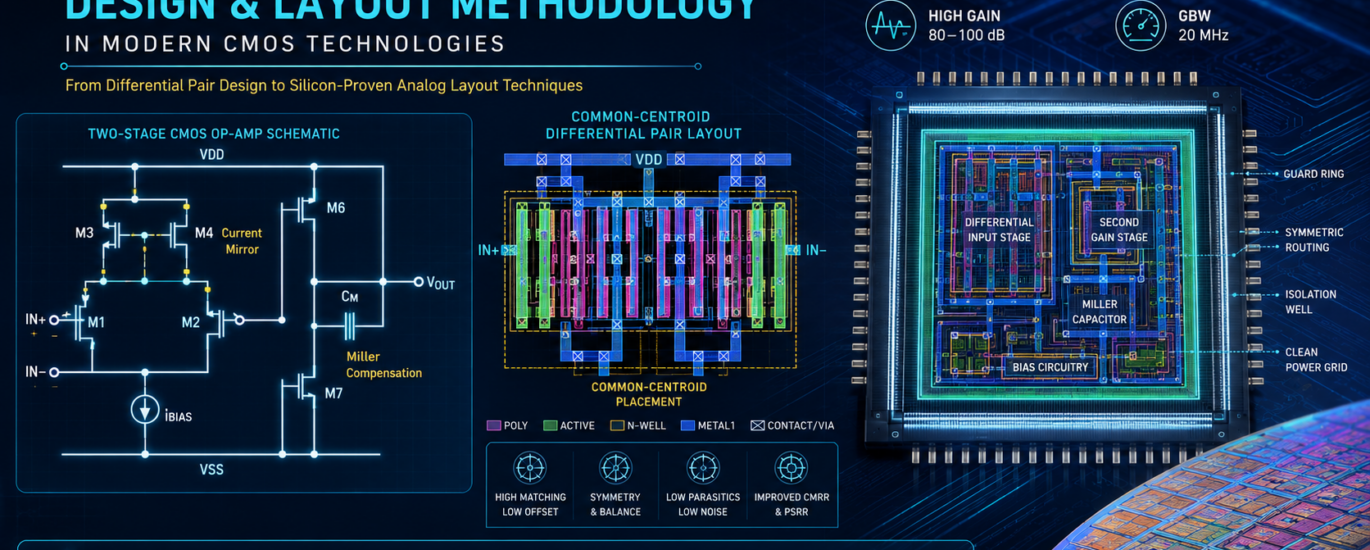
Operational Amplifier Design and Layout Methodology in Modern CMOS Technologies
A comprehensive guide to two-stage CMOS Op-Amp design, analog layout techniques, noise optimization, and post-layout verification — as taught at StarVLSI, Bangalore's best VLSI training institute.
The Operational Amplifier (Op-Amp) remains one of the most fundamental building blocks in analog and mixed-signal integrated circuits. Despite the increasing complexity of modern System-on-Chip (SoC) devices, operational amplifiers continue to be widely used in Analog-to-Digital Converters (ADCs), Digital-to-Analog Converters (DACs), Phase Locked Loops (PLLs), Low Dropout Regulators (LDOs), sensor interfaces, audio circuits, and power management systems.
Designing a high-performance operational amplifier involves much more than achieving gain and bandwidth targets at the schematic level. The physical implementation of the circuit significantly influences offset voltage, noise performance, Common Mode Rejection Ratio (CMRR), Power Supply Rejection Ratio (PSRR), and overall reliability. Consequently, analog layout is often considered an extension of the analog design process rather than a separate activity.
This article discusses the design methodology of a typical two-stage CMOS operational amplifier and the layout techniques required to achieve silicon-proven performance — core skills covered in the AMS Design curriculum at StarVLSI, Bangalore's best VLSI training institute.
Operational Amplifier Performance Targets
A typical CMOS operational amplifier intended for mixed-signal SoC applications may target the following specifications. Meeting these requires careful topology selection, device sizing, bias optimization, compensation design, and layout planning.
| Parameter | Typical Value |
|---|---|
| Supply Voltage | 1.8 V – 3.3 V |
| Open Loop Gain | 80 – 100 dB |
| Gain Bandwidth Product | 20 MHz |
| Phase Margin | > 60° |
| Slew Rate | 10 V/μs |
| Input Offset Voltage | < 2 mV |
| CMRR | > 80 dB |
| PSRR | > 80 dB |
| Power Consumption | < 1 mW |
Selecting the Operational Amplifier Architecture
The first step in analog design is selecting the appropriate architecture. For moderate gain and bandwidth requirements, a two-stage Miller compensated operational amplifier remains one of the most popular choices.
This topology provides a good balance between gain, power consumption, silicon area, and design complexity. The core architecture consists of:
- Differential input stage
- Active load current mirror
- Second gain stage
- Miller compensation network
- Bias generation circuitry
- Output driver stage
Designing the Differential Input Stage
The differential pair is the heart of the operational amplifier because it determines offset voltage, noise performance, and common-mode behavior. The transconductance of the input stage directly affects gain bandwidth and input-referred noise. Designers typically choose large device dimensions to reduce mismatch and flicker noise.
Key design trade-offs: A larger transistor area improves matching and reduces offset but increases parasitic capacitance. Higher bias current improves speed and slew rate but increases power consumption. Longer channel lengths improve gain and output resistance but reduce frequency response. Extensive corner simulations and Monte Carlo analysis determine the optimal transistor dimensions.
Current Mirror and Active Load Design
Current mirrors establish bias currents throughout the amplifier and significantly influence gain accuracy and power supply rejection. The current mirror load converts the differential current generated by the input pair into a single-ended voltage. To maximize gain, long-channel devices are often employed in these structures.
Special attention must be paid to current mirror matching because mismatches directly contribute to offset voltage and gain variation.
Gain Stage and Frequency Compensation
The second stage provides additional gain required to achieve open-loop gains exceeding 80 dB. Without compensation, multiple poles generated by the amplifier stages can lead to instability. Miller compensation introduces a dominant pole that ensures stable closed-loop operation.
The compensation capacitor value is selected carefully to achieve:
- Adequate phase margin
- Sufficient gain bandwidth
- Fast settling time
- Minimal ringing
AC simulations are used extensively during this phase of design optimization.
Noise Optimization
Noise is a major concern in precision analog circuits. Thermal noise arises from transistor channel resistance, while flicker noise becomes significant at low frequencies. The input differential pair contributes the majority of input-referred noise.
To minimize noise, designers typically:
- Increase differential pair area
- Use longer channel devices
- Optimize bias current
- Reduce parasitic coupling
- Employ clean power supplies
Layout Planning Before Physical Design
Before beginning layout, the analog designer and layout engineer jointly create a floorplan. A well-planned floorplan minimizes routing parasitics and simplifies matching requirements. The floorplan identifies:
- Differential pair location
- Current mirror placement
- Compensation capacitor position
- Output stage location
- Bias circuit location
- Power routing strategy
Differential Pair Layout Methodology
The differential pair requires the highest level of matching within the entire amplifier. This arrangement ensures that process gradients affect both devices equally, minimizing offset voltage caused by process variations.
Common-Centroid
Cancels linear process gradients across the die, directly reducing systematic offset voltage.
Interdigitated Fingers
Alternates sub-fingers of both transistors to improve mismatch immunity further.
Dummy Devices
Placed at array edges to equalize the surrounding environment for interior devices.
Symmetrical Routing
Equal wire lengths, equal vias, and equal parasitic capacitance on differential signals.
Routing Considerations in Analog Layout
Unlike digital designs, analog routing must focus on symmetry and parasitic control rather than routing completion. Differential input signals should have equal wire lengths, equal parasitic capacitance, equal metal layers, and equal number of vias.
High-impedance nodes should be routed using the shortest possible paths to minimize unwanted capacitance. The compensation node requires particular care because additional parasitics can significantly alter phase margin.
Guard Ring and Substrate Isolation Techniques
Substrate noise is one of the most common causes of analog performance degradation in mixed-signal systems. To mitigate substrate coupling:
- P+ guard rings are connected to VSS
- N+ guard rings are connected to VDD
- Deep N-Well isolation is used when available
- Sensitive analog blocks are isolated from digital circuits
Power Routing and Reliability Considerations
Power routing impacts gain, PSRR, electromigration reliability, and IR drop. Wide metal traces and multiple vias are employed to reduce resistance. Analog power and ground networks should be separated from noisy digital supplies whenever possible. Reliability verification includes electromigration analysis, IR drop analysis, latch-up verification, and Electrostatic Discharge verification.
Post-Layout Verification and Signoff
Layout completion is only the beginning of the signoff process. The design undergoes a rigorous multi-step verification sequence before tape-out:
Design Rule Check (DRC) — verifies compliance with foundry manufacturing rules, catching minimum spacing, width, and density violations.
Layout Versus Schematic (LVS) — confirms connectivity correctness, ensuring the extracted netlist matches the schematic intent.
Parasitic Extraction (PEX) — models interconnect resistance and capacitance for accurate post-layout simulation.
Post-Layout Simulation — validates gain, bandwidth, phase margin, noise, offset, and power consumption with real parasitics.
Monte Carlo Analysis — verifies robustness against mismatch and process variations across statistical corners.
Tape-out readiness: Only after successful completion of all signoff checks can the amplifier be considered ready for tape-out. At StarVLSI — the best VLSI institute in Bangalore — students practice the complete DRC → LVS → PEX → post-layout sim workflow using industry-standard EDA tools.
Conclusion
The operational amplifier remains one of the most important analog building blocks in modern integrated circuits. Achieving high gain, low offset, low noise, and robust stability requires careful attention to both circuit design and physical implementation.
The analog layout process is not merely a translation of the schematic into geometry — it is an extension of the design itself. Techniques such as common-centroid placement, interdigitated structures, symmetrical routing, guard rings, and substrate isolation often determine whether the final silicon meets its specifications.
As semiconductor technologies continue to scale and mixed-signal integration becomes increasingly complex, the collaboration between analog designers and layout engineers becomes even more critical. A well-designed and carefully laid-out operational amplifier can provide years of reliable operation across a wide range of applications.
Learn Analog IC Design with StarVLSI
At StarVLSI — Bangalore's best VLSI training institute — engineers gain hands-on experience in analog circuit design, CMOS operational amplifiers, current mirrors, bandgap references, PLLs, ADCs, DACs, custom layout techniques, parasitic extraction, and AMS verification flows using industry-standard EDA tools.
Explore AMS Design Courses →