
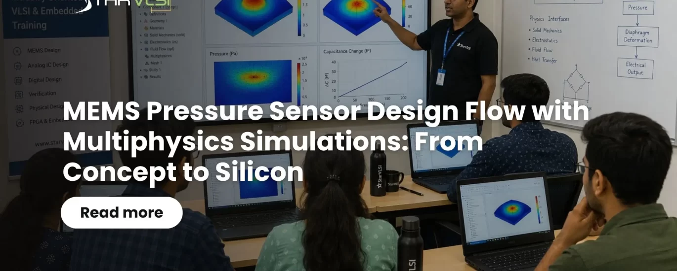
MEMS Pressure Sensor Design Flow with Multiphysics Simulations: From Concept to Silicon
A MEMS pressure sensor converts an external mechanical stimulus into an electrical signal by measuring the deflection of a thin silicon diaphragm. Because the design couples mechanical, electrical, thermal, and fabrication effects together, modern development relies on multiphysics simulation — modeling stress, heat transfer, electrical response, and packaging interactions in one integrated flow — to cut down costly silicon iterations before a single wafer is fabricated.
Micro-Electro-Mechanical Systems (MEMS) pressure sensors have become one of the most widely deployed sensing technologies in modern electronic systems. They are found in automobiles for tire pressure monitoring and engine management, in industrial automation for process control, in medical devices for patient monitoring, and in consumer electronics for altitude measurement and environmental sensing. Their popularity stems from their small size, high sensitivity, low power consumption, and compatibility with standard CMOS manufacturing processes.
Unlike conventional integrated circuits that deal only with electrical signals, MEMS devices integrate microscopic mechanical structures with semiconductor electronics. A pressure sensor converts an external mechanical stimulus into an electrical signal through the deformation of a silicon diaphragm. This interaction between mechanical movement, electrical behavior, thermal effects, and fabrication processes makes MEMS design considerably more complex than traditional IC design.
For this reason, modern MEMS development relies heavily on multiphysics simulations, where multiple physical domains are solved simultaneously. Rather than validating individual aspects independently, engineers model mechanical deformation, stress distribution, heat transfer, electrical characteristics, material behavior, and package interactions together. This integrated simulation methodology dramatically improves design accuracy while reducing costly silicon iterations.
What Is a MEMS Pressure Sensor?
A MEMS pressure sensor measures the pressure exerted by gases or liquids by sensing the minute deflection of a thin silicon diaphragm. When pressure is applied, the diaphragm bends by only a few micrometers, producing mechanical stress within the silicon. Depending on the sensing technology employed, this stress is converted into an electrical output through changes in resistance, capacitance, resonant frequency, or optical characteristics.
Among the available sensing mechanisms, piezoresistive and capacitive sensing dominate commercial products. Piezoresistive sensors employ diffused resistors embedded in the diaphragm that change resistance when mechanical stress is applied. Capacitive sensors measure the variation in capacitance caused by diaphragm displacement relative to a fixed electrode. Both technologies offer excellent performance, although capacitive sensors generally provide lower power consumption while piezoresistive devices offer simpler signal conditioning circuitry.
A complete MEMS pressure sensor integrates the sensing element with analog front-end electronics, analog-to-digital conversion, temperature compensation, calibration memory, digital interfaces, and protective packaging. Consequently, successful sensor development requires close interaction between mechanical design engineers, analog circuit designers, process engineers, and packaging specialists.
The Design Flow at a Glance
The development of a MEMS pressure sensor follows a highly iterative engineering process rather than a simple linear sequence. Each design decision influences subsequent stages, often requiring multiple optimization loops before fabrication begins. Unlike digital integrated circuits, where functionality is verified primarily through logic simulation, MEMS devices require simultaneous verification across several physical domains, making multiphysics simulation indispensable throughout the design flow.
System Specification
Every MEMS project begins by converting the application requirements into specifications. The target operating environment determines the pressure range, measurement accuracy, resolution, response time, power consumption, and long-term reliability targets.
Automotive pressure sensors, for example, must function accurately from −40°C to +150°C while surviving mechanical vibration, thermal cycling, humidity, and electrical disturbances throughout the vehicle's lifetime. Medical sensors demand exceptional precision and stability, whereas industrial sensors often prioritize ruggedness and extended operating pressure ranges.
Clearly defining these requirements at the outset enables designers to select appropriate sensor architectures and avoid costly redesigns later in the development process.
Choosing the Sensing Mechanism
Choosing the sensing principle is one of the most critical architectural decisions in MEMS design. The sensing mechanism determines not only the electrical interface but also the fabrication process, mechanical geometry, packaging requirements, and overall sensor performance.
Piezoresistive sensors remain the preferred choice for automotive, hydraulic, and industrial pressure monitoring because of their mature manufacturing processes, excellent sensitivity, and straightforward analog interface circuitry. Capacitive sensors, on the other hand, are widely adopted in battery-powered portable devices due to their extremely low power consumption and long-term stability.
The final selection depends on application priorities such as sensitivity, power budget, operating environment, manufacturing cost, and expected product lifetime.
Mechanical Structure Design
The diaphragm is the heart of every MEMS pressure sensor. Its dimensions largely determine the sensor's sensitivity, linearity, mechanical robustness, and dynamic response. Engineers carefully optimize diaphragm thickness, width, length, support conditions, and cavity dimensions to achieve the desired pressure response.
Several diaphragm geometries are commonly employed in commercial sensors, including square, circular, rectangular, bossed, and corrugated structures. Each configuration offers different trade-offs between stress distribution, linearity, burst pressure, and fabrication complexity.
Mechanical optimization begins long before silicon fabrication using Finite Element Analysis (FEA), allowing designers to evaluate numerous geometries rapidly while minimizing prototype iterations.
Material Selection
Selecting suitable materials is equally important because material properties directly influence sensor performance throughout. Single-crystal silicon remains the preferred diaphragm material owing to its exceptional mechanical properties, predictable elastic behavior, and compatibility with semiconductor manufacturing.
Additional materials such as silicon dioxide, silicon nitride, aluminum, gold, ceramics, and glass are incorporated to provide insulation, electrical interconnections, passivation, and environmental protection. During simulation, engineers account for each material's Young's modulus, thermal expansion coefficient, density, residual stress, and electrical conductivity to accurately predict device behavior under varying environmental conditions.
Finite Element Analysis
Mechanical Finite Element Analysis represents the first major multiphysics simulation stage in MEMS development. At this stage, engineers apply different pressure loads to the diaphragm and calculate resulting displacement, stress, strain, and structural integrity.
Simulation results identify stress concentration regions, estimate burst pressure limits, evaluate mechanical resonance frequencies, and determine whether the diaphragm satisfies sensitivity and linearity requirements. These analyses often lead to multiple geometry refinements before proceeding to electrical modeling.
Mechanical FEA significantly reduces design risk by replacing numerous fabrication iterations with virtual prototyping.
Electrical Simulation
Once the mechanical behavior is understood, designers investigate how diaphragm deformation translates into electrical signals. In piezoresistive sensors, electrical simulations evaluate resistance changes within the sensing elements and predict Wheatstone bridge output voltages across the complete operating pressure range.
For capacitive sensors, simulations determine capacitance variation resulting from diaphragm movement while accounting for parasitic capacitances, fringe fields, and electrode geometry. Analog circuit simulations then evaluate amplification, filtering, offset compensation, noise performance, and power consumption to ensure that the sensor meets system-level specifications.
The integration of mechanical and electrical simulations enables accurate prediction of overall sensor sensitivity before fabrication.
Thermal Simulation
Temperature significantly influences MEMS pressure sensor accuracy because both silicon properties and electronic circuits exhibit temperature-dependent behavior. Thermal simulations therefore evaluate the effects of ambient temperature variation, self-heating, thermal gradients, and package expansion.
These analyses predict offset drift, sensitivity variation, thermal stress, and long-term stability across the intended operating temperature range. Such simulations are especially critical for automotive applications, where sensors routinely experience wide temperature excursions over many years of operation.
Coupled Electromechanical Simulation
Real MEMS devices never operate under purely mechanical or purely electrical conditions. Mechanical deformation alters electrical parameters, while electrical biasing can influence mechanical forces in certain sensor architectures. Coupled electromechanical simulation simultaneously solves these interacting phenomena to predict actual sensor behavior.
This integrated analysis enables engineers to evaluate pressure sensitivity, non-linearity, hysteresis, dynamic response, and electrical output using realistic operating conditions. Such simulations greatly improve confidence in first-pass silicon performance.
Fluid-Structure Interaction Analysis
Many MEMS pressure sensors operate in environments where gases or liquids directly influence diaphragm dynamics. Fluid-Structure Interaction (FSI) simulations model the interaction between flowing fluids and deformable mechanical structures.
These simulations predict air damping, pressure transients, acoustic coupling, viscous effects, and dynamic response characteristics. Applications such as medical ventilators, hydraulic systems, industrial compressors, and aerospace instrumentation particularly benefit from accurate FSI analysis.
MEMS Process Simulation
Unlike digital integrated circuits, MEMS fabrication physically creates movable three-dimensional structures using specialized micromachining techniques. Process simulation models every fabrication step, including oxidation, ion implantation, diffusion, deep reactive ion etching, wafer bonding, sacrificial layer removal, and cavity formation.
By accurately predicting geometry evolution during fabrication, process simulations enable engineers to identify manufacturing issues before masks are released, significantly reducing development cost and schedule risk.
Packaging Simulation
Packaging is frequently one of the largest contributors to measurement error in MEMS pressure sensors. Mechanical stresses introduced during die attachment, wire bonding, encapsulation, or thermal expansion can exceed the stress generated by the applied pressure itself.
Packaging simulations quantify these effects and guide optimization of die attach materials, package geometry, sealing methods, and thermal expansion compatibility. Proper package design is essential for achieving long-term measurement stability and reliability.
Reliability Analysis
MEMS pressure sensors are expected to operate reliably for more than a decade in harsh environments. Reliability simulations evaluate fatigue, thermal cycling, vibration, mechanical shock, humidity exposure, material aging, and package degradation under accelerated stress conditions.
These analyses allow engineers to identify potential failure mechanisms before fabrication and ensure compliance with demanding automotive and industrial qualification standards.
Electronics Co-Design
Modern MEMS pressure sensors are no longer standalone sensing elements but complete smart sensor systems. They integrate precision analog amplifiers, programmable gain stages, sigma-delta analog-to-digital converters, digital calibration engines, embedded memory, temperature compensation circuits, and communication interfaces such as I²C, SPI, SENT, LIN, or CAN.
Designing the MEMS structure and electronic circuitry together ensures optimal performance while minimizing noise, offset, and power consumption. This co-design methodology has become standard practice for highly integrated automotive and industrial sensors.
Verification and Physical Validation
Before fabrication, the complete design undergoes extensive verification to ensure manufacturability and functionality. MEMS layouts are checked for process compatibility, mechanical constraints, and fabrication rules. Standard IC verification methods such as Design Rule Checking (DRC) and Layout Versus Schematic (LVS) are combined with MEMS-specific process validation and assembly verification.
This comprehensive verification flow minimizes manufacturing risks and significantly improves first-pass fabrication success.
Multiphysics Simulation Tools Used in Industry
The complexity of MEMS pressure sensor development has led to the adoption of sophisticated simulation platforms that integrate multiple engineering disciplines.
| Tool | Primary Use |
|---|---|
| COMSOL Multiphysics | Simultaneous structural, thermal, electrical, and fluidic simulation in one environment |
| ANSYS Mechanical / Fluent | Structural and fluid dynamics analysis |
| Cadence CoventorMP | MEMS process and device simulation |
| IntelliSuite | MEMS design, process, and simulation |
| Synopsys Sentaurus | TCAD-level device and process simulation |
| Silvaco Victory Process | Semiconductor process simulation |
| Cadence Virtuoso | Analog/mixed-signal electronics co-design |
| Siemens Simcenter | Multiphysics and system-level simulation |
Design Challenges
Despite significant advances in simulation technology, MEMS pressure sensor development remains a multidisciplinary engineering challenge. Achieving high sensitivity often requires extremely thin diaphragms that are susceptible to nonlinear deformation and mechanical failure. Fabrication-induced residual stress can alter diaphragm flatness, while packaging introduces additional mechanical stress that may dominate the actual sensing signal. Temperature variation, process tolerances, and material aging further complicate sensor calibration and long-term stability.
These challenges highlight why multiphysics simulation is no longer optional but an essential component of modern MEMS product development.
Future Trends
The next generation of MEMS pressure sensors is moving toward intelligent, highly integrated sensing platforms. Artificial intelligence is increasingly being applied to optimize diaphragm geometry, automate design exploration, and accelerate calibration. Digital twins enable virtual representation of complete sensor lifecycles, allowing engineers to predict aging, manufacturing variation, and field performance before production.
Wafer-level packaging, heterogeneous integration, embedded RISC-V processors, and edge AI capabilities are transforming pressure sensors into smart autonomous sensing nodes capable of local processing, self-diagnostics, predictive maintenance, and secure communication. These technologies are expected to play a significant role in Industry 4.0, autonomous vehicles, smart healthcare, and next-generation IoT ecosystems.
Conclusion
Designing a MEMS pressure sensor requires seamless integration of mechanical engineering, semiconductor processing, analog electronics, packaging technology, and reliability engineering. Unlike traditional integrated circuit development, MEMS design demands continuous interaction between multiple physical domains throughout the entire design cycle.
Multiphysics simulations have fundamentally transformed MEMS development by enabling engineers to evaluate mechanical deformation, electrical response, thermal behavior, fabrication effects, fluid interactions, and packaging stresses within a unified virtual environment. This comprehensive simulation approach significantly shortens development cycles, reduces fabrication iterations, lowers costs, and dramatically improves the probability of first-pass silicon success.
As semiconductor technology continues to evolve toward smarter, safer, and more connected systems, expertise in MEMS design and multiphysics simulation will become an increasingly valuable skill for engineers developing the next generation of intelligent sensing solutions.
Frequently Asked Questions
A MEMS pressure sensor measures the pressure exerted by gases or liquids by sensing the deflection of a thin silicon diaphragm, converting that mechanical deformation into an electrical signal through changes in resistance, capacitance, resonant frequency, or optical properties.
Piezoresistive sensors use diffused resistors that change resistance under mechanical stress and offer simpler signal conditioning. Capacitive sensors measure capacitance changes from diaphragm displacement and generally consume less power, making them popular in battery-powered devices.
MEMS devices couple mechanical, electrical, thermal, and fabrication effects together, so multiphysics simulation lets engineers validate all of these domains simultaneously, improving design accuracy and reducing costly silicon iterations.
The flow typically covers system specification, sensing mechanism selection, mechanical structure design, material selection, finite element analysis, electrical and thermal simulation, coupled electromechanical and fluid-structure analysis, process and packaging simulation, reliability analysis, electronics co-design, and final verification.
Common industry tools include COMSOL Multiphysics, ANSYS Mechanical and Fluent, Cadence CoventorMP, IntelliSuite, Synopsys Sentaurus, Silvaco Victory Process, Cadence Virtuoso, and Siemens Simcenter.
Learn Advanced MEMS Design with StarVLSI
At StarVLSI, we provide industry-oriented training in various domains. Our courses emphasize hands-on learning with industry-standard EDA tools, practical design methodologies, and real-world projects to prepare engineers for successful careers in the semiconductor industry.
Explore Our Training ProgramsStay connected with the StarVLSI Blog for more in-depth technical articles on emerging semiconductor technologies, and explore our training programs to build expertise in cutting-edge technologies.