
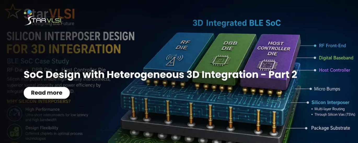
SoC Design with Heterogeneous 3D Integration — Part 2
In Part 1, we covered why chiplet-based heterogeneous integration makes sense for a three-die BLE SoC, and walked through the silicon interposer, TSVs, floorplanning, routing strategy, and power delivery network design. In this concluding Part 2, we look at clock distribution, signal integrity, thermal management, the complete design flow, verification methodology, manufacturing challenges, and where the technology is heading next.
Clock Distribution Across Multiple Chiplets
Clock distribution in chiplet-based architecture presents unique challenges because multiple dies must operate synchronously while maintaining extremely low jitter and skew. Although routing distances inside the interposer are relatively short, clock quality remains one of the most important determinants of overall system performance.
The BLE SoC contains several independent clock domains. A low-frequency sleep oscillator supports low-power standby operation, while a high-precision crystal oscillator provides the RF reference clock. The PLL generates the RF carrier frequency, the Digital Baseband executes packet processing using a high-speed system clock, and the Host Controller processor typically operates from an independent CPU clock.
These clocks may either originate from one die and be distributed through the interposer or be generated independently and synchronized using clock-domain crossing logic.
Clock routing follows strict design rules. Differential clock pairs are shielded using adjacent ground lines, routing lengths are carefully matched to reduce skew, and clock nets are isolated from high-current power switching regions to minimize injected jitter. In advanced designs, dedicated clock routing layers within the interposer provide additional shielding and reduce coupling with data signals.
Engineers also perform Clock Tree Synthesis (CTS) at the package level, ensuring that timing closure extends beyond individual dies and encompasses the entire heterogeneous system.
Signal Integrity Analysis: Ensuring Reliable High-Speed Communication
Although silicon interposers provide excellent electrical performance, high-speed communication between chiplets still requires extensive Signal Integrity (SI) analysis. As operating frequencies increase into multi-gigabit ranges, even small discontinuities in impedance or trace geometry can introduce reflections, crosstalk, and eye closure.
The RF die exchanges sensitive analog control signals with the Digital Baseband, while wide digital interfaces transfer continuous streams of packet data. These signals coexist within the same routing environment and therefore require careful electromagnetic isolation.
Engineers perform detailed SI simulations to evaluate insertion loss, return loss, propagation delay, impedance discontinuities, and crosstalk between neighboring traces. Differential pairs are designed with tightly controlled spacing, while reference ground planes ensure predictable return current paths.
For RF-related signals, electromagnetic (EM) simulation tools model the complete interposer structure, including TSVs, micro-bumps, metal layers, and package parasitics. This allows designers to predict performance before fabrication and optimize routing geometries for maximum signal quality.
By integrating SI analysis early in the design cycle, engineers can avoid expensive redesigns caused by package-level communication failures.
Thermal Analysis and Heat Management in 3D Integration
One of the primary engineering challenges introduced by chiplet-based architecture is thermal management. While partitioning a system into multiple dies improves manufacturing yield and technology optimization, it also concentrates power within a relatively small package area.
In the BLE SoC example, the RF Power Amplifier generates significant heat during wireless transmission. The Digital Baseband continuously executes packet processing algorithms, encryption engines, and error correction logic, while the Host Controller processor contributes dynamic switching power during protocol execution.
Without careful thermal planning, localized hot spots may develop beneath high-power chiplets, degrading device reliability, increasing leakage current, and reducing operating frequency.
Thermal-aware floorplanning therefore becomes an integral part of the interposer design process. High-power chiplets are separated wherever possible, while TSV arrays assist vertical heat conduction through the silicon interposer into the package substrate. Additional heat spreaders and thermal interface materials are incorporated within the package to improve overall cooling performance.
Modern design flows include multi-physics simulations that simultaneously analyze electrical, thermal, and mechanical behavior. These simulations help identify thermal bottlenecks before manufacturing begins, allowing engineers to optimize chiplet placement and package construction.
Complete Silicon Interposer Design Flow
Designing a silicon interposer requires close collaboration among IC designers, package engineers, signal integrity specialists, thermal engineers, and manufacturing teams. Unlike traditional SoC development, where chip and package are often designed independently, heterogeneous integration demands concurrent co-design of all system components.
This multidisciplinary workflow requires extensive collaboration between EDA tools supporting IC implementation, package layout, electromagnetic simulation, thermal analysis, and mechanical stress evaluation.
Verification Methodology for Silicon Interposer Designs
Verification extends well beyond conventional RTL simulation when designing heterogeneous chiplet systems. Each individual die undergoes functional verification independently, but complete system validation must also account for package-level interactions introduced by the silicon interposer.
Electrical verification includes Design Rule Checking (DRC), Layout Versus Schematic (LVS), parasitic extraction, static timing analysis, and power integrity verification. Interposer-specific checks ensure TSV connectivity, bump alignment, routing continuity, and manufacturability.
Engineers perform package-aware timing analysis by incorporating interposer parasitics into static timing models. Electromagnetic simulations verify RF performance, while thermal simulations evaluate temperature distribution across all chiplets.
Mechanical simulations assess stresses resulting from differences in the Coefficient of Thermal Expansion (CTE) between silicon, solder bumps, underfill materials, and organic substrates. Reliability verification includes electromigration analysis, bump fatigue prediction, thermal cycling qualification, and TSV stress evaluation.
Only after successfully completing these multidisciplinary verification steps is the heterogeneous package considered ready for manufacturing.
Manufacturing Challenges and Reliability Considerations
Although silicon interposer technology offers remarkable performance advantages, manufacturing introduces several unique challenges that designers must understand during the architecture phase.
Micro-bump alignment between chiplets and the interposer requires sub-micron placement accuracy. Any misalignment may result in open circuits or increased contact resistance. Through Silicon Via fabrication involves deep silicon etching, dielectric isolation, copper filling, and chemical mechanical polishing, each of which contributes to manufacturing complexity and cost.
Mechanical stresses caused by repeated thermal cycling can fatigue solder joints over the product lifetime. Differences in thermal expansion between chiplets, interposer silicon, package substrate, and PCB generate stress concentrations that must be minimized through careful material selection and structural design.
Yield management also becomes increasingly important because multiple independently fabricated chiplets must all function correctly before assembly. Fortunately, chiplet architecture allows Known Good Die (KGD) testing prior to packaging, significantly improving overall manufacturing yield compared to large monolithic SoCs.
Emerging Trends in Silicon Interposer Technology
The semiconductor industry is rapidly evolving beyond passive silicon interposers toward increasingly intelligent packaging platforms. Active interposers containing embedded clock distribution, power management, monitoring circuits, and network-on-chip routers are already under development for next-generation heterogeneous computing systems.
Standardized die-to-die communication protocols such as Universal Chiplet Interconnect Express (UCIe) are enabling interoperable chiplets from different vendors, paving the way for a modular semiconductor ecosystem. Optical interconnects, silicon photonics, and embedded voltage regulators are expected to become integral components of future interposer-based designs.
For wireless and IoT applications, future packages are likely to integrate BLE, Wi-Fi, Ultra-Wideband (UWB), GNSS, AI accelerators, sensor interfaces, and security processors into unified chiplet platforms. This level of integration will significantly reduce product development time while allowing independent technology evolution for each subsystem.
As these technologies mature, expertise in advanced packaging will become just as important as expertise in RTL design, physical implementation, and verification.
Conclusion
Silicon interposers have fundamentally transformed the way modern semiconductor systems are designed by enabling heterogeneous integration of independently optimized chiplets within a single package. Rather than forcing RF, digital, memory, and processor subsystems into a common process technology, designers can now partition complex systems into specialized dies while preserving the performance advantages of short, high-density interconnections.
Through the BLE SoC case study presented across this two-part series, we have demonstrated how an RF Front-End die, Digital Baseband die, and Host Controller die can be efficiently integrated using a silicon interposer. Beyond simply providing electrical connectivity, the interposer serves as the foundation for power delivery, clock distribution, thermal management, and high-speed communication, making it a critical component of the overall system architecture.
Successful interposer design demands a multidisciplinary engineering approach that combines semiconductor device physics, package engineering, signal integrity, power integrity, thermal analysis, mechanical reliability, and advanced EDA methodologies. As chiplet-based architecture continues to gain widespread adoption across wireless communication, automotive electronics, AI accelerators, networking equipment, and edge computing, engineers with expertise in silicon interposer design will be increasingly valuable to the semiconductor industry.
Master Advanced Packaging with StarVLSI
At StarVLSI, we believe that mastering advanced packaging technologies is essential for the next generation of VLSI professionals. Through comprehensive training, industry-oriented projects, and hands-on exposure to modern EDA tools, StarVLSI prepares aspiring semiconductor engineers to address the evolving challenges of 3D integration and advanced chiplet-based system design.
Explore StarVLSI CoursesPart 2 of 2 — StarVLSI Blog. Stay connected with the StarVLSI Blog for more in-depth articles on advanced VLSI design, semiconductor packaging, RF systems, physical design, verification methodologies, and emerging technologies shaping the future of the semiconductor industry.