Why the Next Generation of SoC Designers Must Be Science-Centric, Not Tool-Centric, in the AI Era
AI-enabled EDA is starting to automate RTL generation, verification, optimization, and physical implementation — tasks that used to define "knowing the tools." That doesn't make engineering knowledge less important; it makes it more important. This article argues that the next generation of SoC designers needs a foundation in physics, chemistry, and mathematics first, with AI and EDA tools sitting above that foundation as accelerants — not as the core skill itself.
The Semiconductor Is a Physics-Based System
The semiconductor industry is entering a fundamental transition. For decades, VLSI design education and professional training have focused heavily on learning EDA tools, design flows, modeling languages, simulators, synthesis, place-and-route, verification environments and implementation methodologies. These skills remain useful, but Artificial Intelligence is beginning to change their relative importance.
AI-enabled design environments can increasingly automate RTL generation, verification, optimization, modeling, constraint generation, physical implementation and even portions of architecture exploration. Trained AI models can learn patterns from decades of successful designs and assist designers in performing tasks that previously required extensive hands-on knowledge of individual EDA tools.
This does not make engineering knowledge less important. It makes fundamental engineering knowledge more important.
The next generation of SoC designers will need to understand not only how to design something, but why the system behaves the way it does. They must understand the physical principles governing semiconductor devices, the chemistry behind materials and fabrication, and the mathematics required to describe, analyze and optimize complex systems. For the next generation of VLSI education, the emphasis therefore needs to shift from "learning tools" to "learning science and engineering, with AI as the design assistant."
At its most fundamental level, every SoC is a physical system. The transistor is governed by semiconductor physics. Interconnects are governed by electromagnetic and electrical principles. Memories depend on charge storage and device characteristics. Sensors convert physical phenomena into electrical signals. RF circuits depend on electromagnetic behavior. Power delivery is governed by electrical and thermal principles. Clock networks experience propagation delay, variation and jitter because of physical effects.
Digital abstraction hides much of this complexity, but it does not eliminate it. A designer writing RTL may think in terms of logic values, registers and transactions. Silicon, however, operates with voltages, currents, electric fields, capacitance, resistance, temperature, carrier mobility, leakage and noise. This distinction becomes increasingly important as SoCs move toward advanced process nodes, heterogeneous integration, chiplets, 3D integration, high-speed interfaces, AI accelerators and sensor-rich systems. The designer who understands the underlying physics can recognize when an apparently correct model is physically unrealistic.
Physics as a Core Skill for SoC Designers
Physics should not be treated as a subject that ends after undergraduate engineering education. It needs to become an active engineering skill throughout a VLSI career.
A designer working on a high-speed interface needs to understand transmission lines, impedance, reflections, crosstalk and electromagnetic coupling. A designer working on an RF SoC needs knowledge of electromagnetic fields, noise, oscillators, resonance and frequency-domain behavior. A designer working on automotive SoCs needs to understand temperature effects, reliability and device variation. Similarly, low-power design requires an understanding of the physical origins of dynamic power, leakage power, capacitance and voltage scaling.
Thermal management is another example. An AI accelerator can contain billions of transistors switching at high frequency. Understanding temperature generation and heat transfer becomes essential when designing the architecture and packaging, not merely during post-layout analysis.
The future designer therefore needs to ask questions such as: what physical phenomenon produces this behavior, what parameters control it, how does scaling change it, and what assumptions are hidden inside my model? These questions cannot be answered merely by knowing which EDA environment to open.
Chemistry: The Forgotten Foundation of Semiconductor Engineering
Chemistry is often absent from conventional VLSI design discussions, yet modern semiconductor technology is deeply dependent on it. The semiconductor manufacturing process involves materials, chemical reactions, deposition, etching, oxidation, diffusion, implantation, lithography, cleaning and contamination control. The electrical properties of the final transistor are strongly influenced by the materials and processes used to manufacture it.
As semiconductor technology evolves, this connection becomes even stronger. Advanced transistor structures, high-k dielectrics, metal gates, new channel materials, advanced interconnect materials, wafer bonding, heterogeneous integration and 3D packaging all require understanding of material properties and chemical processes.
For SoC designers, this knowledge does not mean becoming a semiconductor process chemist. Rather, designers need sufficient understanding to appreciate how material and process choices influence electrical behavior, reliability, temperature characteristics and manufacturing variation — particularly for designers working across the boundary between IC design, packaging and system engineering. The next generation of training programs should therefore introduce semiconductor chemistry and materials science as practical engineering subjects rather than treating them as disconnected academic topics.
Mathematics: The Language Behind Every Modern SoC
If physics explains how the semiconductor behaves and chemistry explains the materials and processes involved, mathematics provides the language used to model and optimize the entire system.
Digital design itself is built on Boolean algebra, discrete mathematics and logic theory. But modern SoC design extends far beyond these fundamentals. Signal processing depends on Fourier analysis, transforms, convolution, sampling theory and filtering. Communications systems depend on probability, statistics, information theory and stochastic processes. Control systems depend on differential equations and system theory. Machine learning depends heavily on linear algebra, probability, optimization and numerical methods.
Physical design involves graph theory, computational geometry, optimization and numerical algorithms. Timing analysis depends on mathematical models of delay and variation. Power analysis involves statistical and numerical modeling. Verification increasingly depends on constrained randomization, probability, formal methods and mathematical reasoning. AI-enabled design itself is fundamentally mathematical.
Therefore, a SoC designer who understands the mathematics behind a model will be better positioned to evaluate AI-generated results rather than simply accepting them.
AI Changes the Role of the Designer — It Does Not Eliminate Engineering
A common misunderstanding about AI-enabled EDA is that AI will replace semiconductor engineers. A more realistic transformation is that AI will replace or automate parts of the engineering workflow.
An AI model may generate an RTL block. Another model may construct a verification environment. An optimization engine may explore architectural alternatives. An AI agent may generate constraints or recommend physical implementation strategies. But the fundamental engineering question remains: is the generated solution actually correct for the intended physical system?
AI can generate a mathematically valid model that does not represent the real system accurately. It can optimize the wrong objective. It can make assumptions that are inappropriate for a particular process, operating condition or application. Human expertise is therefore moving upward — from executing individual design tasks toward defining requirements, selecting assumptions, interpreting results, identifying physical limitations and making engineering decisions.
The New Skill Pyramid for SoC Designers
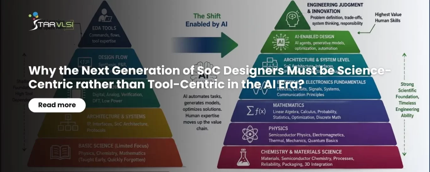
The traditional skill pyramid has often placed EDA tools and implementation methodologies at its center. The AI-enabled design environment suggests a different pyramid — built from the ground up:
Modeling Skills Still Matter, but Their Nature Will Change
Modeling will remain important, but the designer's role in modeling will evolve. Today, engineers may spend considerable time developing detailed models manually. In an AI-enabled environment, trained models can potentially generate portions of these models automatically.
The important human skill will become model formulation and model validation. A designer should know what needs to be modeled, which parameters are important, what assumptions are acceptable, what boundary conditions apply and whether the resulting model corresponds to physical reality.
For example, an AI system may generate a temperature-sensor model. The engineer must still understand temperature-dependent resistance, sensitivity, non-linearity, noise, process variation and calibration requirements. The designer does not necessarily need to manually construct every equation or simulation environment — the designer needs to understand what the equations mean and whether the model represents reality.
From EDA Tool Expertise to Engineering Intent
This transformation does not mean EDA tools are unimportant. EDA tools will continue to be essential for implementation, simulation, verification, synthesis, physical design and signoff. However, memorizing tool commands should no longer be considered the defining characteristic of a highly skilled SoC engineer.
A future engineer should be able to describe the engineering intent clearly enough for an AI-enabled environment to assist with implementation — the question itself needs to change:
"Which command should I use to perform this optimization?"
"What physical or architectural objective am I trying to optimize, what constraints govern it, and how can I prove the implementation satisfies them?"
That is a much higher level of engineering.
Learning From Decades of Silicon Experience
One of the most valuable resources for the next generation of VLSI designers is not another tutorial tool. It is the accumulated experience of engineers who have designed, verified, fabricated, debugged and brought silicon products to market over several decades.
Experienced engineers have learned lessons that are rarely captured completely in textbooks. They understand why certain architectures fail in silicon despite appearing correct in simulation. They recognize the importance of margins, corner cases, process variation, thermal behavior, packaging limitations, clock interactions and system-level effects.
AI provides an opportunity to capture and transfer this knowledge at unprecedented scale. Training programs should therefore combine fundamental science with decades of practical engineering experience and use AI to make that knowledge accessible to the next generation.
What Should a Future VLSI Training Curriculum Look Like?
A future-oriented VLSI curriculum should begin with a strong foundation in physics, chemistry and mathematics and progressively connect these subjects to semiconductor and SoC engineering — not taught as independent, disconnected subjects, but continuously tied to practical semiconductor examples.
Students can learn Fourier transforms through ADC and RF applications, probability through timing and manufacturing variation, thermal physics through processor design, electromagnetics through high-speed interfaces and chemistry through semiconductor fabrication. This approach creates engineers who understand the connection between science → device → circuit → architecture → SoC → system.
Project-Based Learning Should Replace Tool-Centric Training
Instead of spending months teaching students a sequence of EDA commands, training should revolve around complete engineering problems:
EDA tools would naturally appear in these projects, but they would be a means to solve an engineering problem rather than the subject itself.
The Importance of Asking the Right Questions
The greatest advantage of being a scientifically trained designer in an AI-enabled environment will be the ability to ask the right questions. AI can generate answers extremely quickly — the engineer must determine whether the question was formulated correctly in the first place. A strong SoC designer should be able to ask:
These are questions rooted in engineering fundamentals, not EDA tool knowledge.
AI and Human Expertise Will Form the New Design Partnership
The future is not likely to be "AI versus engineers." It is more appropriately understood as AI plus scientifically trained engineers.
AI is exceptionally effective at processing large amounts of information, recognizing patterns, exploring alternatives, generating models and automating repetitive activities. Human engineers remain essential for defining intent, understanding physical reality, evaluating trade-offs, recognizing unusual behavior and taking responsibility for engineering decisions.
A New Philosophy for StarVLSI Training
StarVLSI can play an important role in this transition by developing training programs around science-driven VLSI engineering. The objective should not simply be to produce engineers who can operate today's EDA tools — tools will evolve rapidly, and AI will increasingly automate their usage. The objective should be to create engineers who can remain effective even when the tools change.
A StarVLSI-trained designer should understand the science behind semiconductor behavior, the mathematics behind system models, the materials and chemistry behind manufacturing, the architecture of modern SoCs and the engineering principles required to convert requirements into silicon. EDA tools and AI environments can then be introduced as powerful instruments that accelerate this knowledge, making training resilient to technological change.
The VLSI Engineer of the Future
The VLSI engineer of the future will be neither purely a circuit designer nor merely an EDA-tool specialist. The engineer will increasingly become a science-driven system architect and AI-assisted problem solver — one who understands enough physics to recognize physical limitations, enough chemistry to understand material and manufacturing implications, enough mathematics to formulate and evaluate models, enough electronics to understand circuits and enough architecture knowledge to build complex SoCs.
AI will provide the computational horsepower and automation. EDA tools will provide the implementation infrastructure. But engineering knowledge will continue to define what should be built and whether the result is truly correct.
Conclusion: Teach Science, Let AI Handle the Routine
The semiconductor industry has spent decades developing increasingly sophisticated EDA tools. The next transformation will be driven by AI-enabled design environments capable of automating many tasks that once required extensive tool-specific expertise. This should change the way we train VLSI engineers.
Instead of asking the next generation to spend most of their effort learning the mechanics of tools and flows, we should teach them the foundations that remain valuable regardless of how the tools evolve:
The real competitive advantage of the next generation of SoC designers will not be their ability to remember hundreds of tool commands. It will be their ability to understand a problem deeply, formulate it scientifically, challenge an AI-generated solution and make the right engineering decision.
The future of VLSI education is therefore not less science because of AI, but more science because of AI.
Learn VLSI the Science-Centric Way with StarVLSI
StarVLSI builds training around the physics, chemistry, mathematics, and architecture that stay valuable no matter how EDA tools and AI evolve.
Explore StarVLSI CoursesStay connected with the StarVLSI Blog for more in-depth articles on current and future trends shaping the semiconductor industry.