Guidelines for 3D Integration Architecture of an IoT SoC
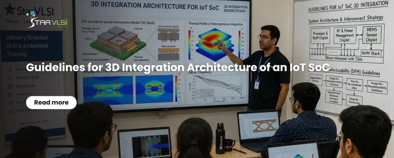
3D integration partitions an IoT SoC into independently optimized chiplets — processor, RF front-end, sensor ASIC, and application host — fabricated on the process technology best suited to each function and connected through high-bandwidth, low-latency die-to-die interconnects such as TSVs, hybrid bonding, or UCIe. This approach improves yield, reduces power, and shortens development cycles compared to monolithic SoC designs.
The rapid growth of Artificial Intelligence (AI), Industrial IoT (IIoT), smart healthcare, automotive electronics, and edge computing is driving a fundamental shift in semiconductor integration. Traditional monolithic System-on-Chip (SoC) architectures are becoming increasingly difficult to scale because advanced CMOS technology nodes are expensive, analog circuits do not always benefit from transistor scaling, and heterogeneous intellectual property (IP) often requires different manufacturing processes. As a result, semiconductor companies are increasingly adopting three-dimensional (3D) integration and chiplet-based architectures to combine independently optimized silicon dies into a single high-performance package.
For Internet of Things (IoT) platforms, 3D integration enables the processor subsystem, RF front end, sensor ASIC, memory, power management, and application processing subsystems to be fabricated using the most suitable semiconductor technologies while communicating through high-bandwidth, low-latency interconnects. This heterogeneous integration approach improves system performance, reduces power consumption, shortens development cycles, and simplifies technology migration.
Evolution from Monolithic SoCs to 3D Integrated Systems
Traditional SoCs integrate every subsystem onto a single silicon die. Although this approach minimizes package complexity, it introduces several design challenges. Large die sizes reduce manufacturing yield, increase fabrication cost, complicate timing closure, and limit technology selection for analog, RF, and sensor interfaces.
Three-dimensional integration addresses these limitations by partitioning the complete system into multiple functional chiplets interconnected through Through-Silicon Vias (TSVs), hybrid bonding, silicon interposers, or advanced package substrates. Each die can be fabricated using the most appropriate process technology while preserving a unified system architecture.
For IoT devices, this approach allows digital processors to utilize advanced FinFET technologies while RF circuits, analog front ends, MEMS interfaces, and sensor ASICs remain on mature mixed-signal processes that offer superior analog performance and lower manufacturing costs.
Typical 3D Architecture for an IoT SoC
A modern IoT platform typically consists of multiple vertically integrated silicon dies organized according to functional specialization. The processor subsystem forms the computational engine and executes the operating system, communication stacks, AI inference algorithms, security services, and application software. The RF front-end die implements Bluetooth LE, Wi-Fi, Thread, Matter, Zigbee, Ultra-Wideband, or cellular connectivity depending on the target application.
The sensor ASIC die interfaces directly with MEMS pressure sensors, gas sensors, temperature sensors, humidity sensors, inertial measurement units, biosensors, or imaging sensors. This subsystem performs analog signal conditioning, amplification, analog-to-digital conversion, calibration, digital filtering, and local signal processing before transferring data to the processor subsystem.
The application host subsystem manages user applications, graphical interfaces, cloud connectivity, local databases, security management, and high-level analytics. Depending on system requirements, this subsystem may execute Linux, Android, Zephyr, FreeRTOS, or proprietary real-time operating systems.
High-bandwidth die-to-die interconnects provide communication between these independently optimized chiplets while maintaining low latency and low power consumption.
Processor Subsystem Design Guidelines
The processor subsystem serves as the central control engine of the entire IoT platform. Modern architectures increasingly adopt configurable RISC-V processor cores because of their scalability, open architecture, and ecosystem flexibility. Depending on application complexity, the processor subsystem may consist of one or more application cores, real-time cores, AI accelerators, and digital signal processors connected through a Network-on-Chip (NoC).
The architecture should incorporate multiple clock domains, dynamic voltage and frequency scaling, secure boot, cryptographic accelerators, hardware root of trust, memory protection, interrupt controllers, DMA engines, cache coherency mechanisms, and hardware virtualization where required. The processor subsystem should also support efficient communication with external chiplets while minimizing interconnect latency and synchronization overhead.
RF Front-End Integration Guidelines
Wireless communication remains one of the most critical functions within IoT systems. The RF subsystem should be isolated from digital switching noise through careful floor planning, dedicated power domains, and package-level shielding. Since RF circuits often require specialized analog semiconductor processes, implementing the RF front end as an independent chiplet significantly improves yield and analog performance.
The RF die should integrate low-noise amplifiers, power amplifiers, mixers, frequency synthesizers, PLLs, ADCs, DACs, baseband processors, and digital calibration engines. Digital interfaces between the processor and RF subsystem should support deterministic timing while minimizing latency during Bluetooth Low Energy, Wi-Fi, Matter, or Ultra-Wideband communication.
Thermal isolation, impedance-controlled routing, antenna matching, electromagnetic compatibility, and coexistence with multiple wireless protocols should be considered early during system architecture development.
Sensor ASIC Architecture Guidelines
Sensor ASICs represent another ideal candidate for heterogeneous integration because they combine precision analog circuits with digital signal processing. Modern sensor ASICs interface with pressure sensors, gas sensors, temperature sensors, humidity sensors, biosensors, and MEMS devices using application-specific analog front ends optimized for low noise and high accuracy.
The architecture should incorporate programmable gain amplifiers, sigma-delta or successive approximation ADCs, reference generators, calibration engines, digital filters, temperature compensation algorithms, sensor diagnostics, built-in self-test functions, and embedded controllers for autonomous sensor management.
Performing local signal processing within the sensor chiplet reduces communication bandwidth while minimizing processor workload and improving overall system energy efficiency.
Application Host Subsystem Architecture
The application host subsystem executes software frameworks responsible for user interaction, cloud communication, device management, over-the-air firmware updates, AI orchestration, data visualization, and application security. Depending on the application domain, this subsystem may execute embedded Linux, Android Automotive, Zephyr, or commercial real-time operating systems.
The architecture should support high-speed memory interfaces, secure storage, virtualization, multimedia processing, graphics acceleration, networking protocols, cloud authentication, and standardized application programming interfaces for edge AI deployment.
Separating application processing from real-time control simplifies software development while allowing independent scalability of application complexity.
Die-to-Die Communication Architecture
Efficient communication between chiplets determines the overall performance of a 3D integrated system. Modern die-to-die interfaces must deliver high bandwidth, deterministic latency, low power consumption, and protocol independence while maintaining compatibility across semiconductor technologies.
Emerging standards such as UCIe, BoW, and proprietary low-power die-to-die interfaces enable scalable communication between independently fabricated chiplets. These interfaces should support packet-based communication, flow control, error detection, retry mechanisms, clock synchronization, power management, and quality-of-service mechanisms for real-time applications.
Designers should partition communication traffic according to latency sensitivity, bandwidth requirements, and functional isolation to maximize system performance.
Memory Architecture Considerations
Memory hierarchy significantly influences IoT system performance. Each chiplet should contain local SRAM optimized for deterministic operation, while shared memory regions facilitate inter-chiplet communication. Larger systems may integrate stacked LPDDR, HBM, or embedded non-volatile memory depending on application requirements.
Memory protection units, cache coherency, DMA optimization, ECC protection, secure memory regions, and low-power retention modes should be incorporated throughout the architecture to improve reliability and energy efficiency.
Power Management Architecture
Power consumption remains one of the most critical design objectives for IoT products. Each chiplet should implement independent power domains with fine-grained clock gating, power gating, voltage scaling, and retention modes. Intelligent power management controllers should dynamically activate only the functional blocks required for current workloads.
Thermal Management in 3D Integration
Stacking multiple active silicon dies increases thermal density and complicates heat removal. Thermal-aware architecture planning therefore becomes an essential component of 3D integration. High-power processor cores should be positioned close to heat spreaders, while temperature-sensitive analog and RF circuits should be thermally isolated whenever possible.
Dynamic thermal management algorithms, distributed temperature sensors, adaptive clock scaling, workload migration, and package-level thermal simulation should be incorporated early in the design process to ensure reliable operation under worst-case conditions.
Functional Safety and Reliability
Many industrial and automotive IoT platforms require compliance with functional safety standards such as ISO 26262 and IEC 61508. Safety-oriented architectures should incorporate redundant communication paths, watchdog timers, ECC-protected memories, clock monitors, voltage supervisors, logic built-in self-test (LBIST), programmable built-in self-test (PBIST), fault management controllers, and comprehensive diagnostic reporting.
Inter-chiplet communication should include cyclic redundancy checks, packet retransmission, timeout detection, and fault isolation mechanisms to maintain reliable operation under transient or permanent failure conditions.
Security Architecture
Security must extend across every chiplet within the integrated system. Hardware root of trust, secure boot, authenticated firmware updates, encrypted die-to-die communication, physically unclonable functions (PUFs), secure key storage, cryptographic accelerators, secure debug interfaces, and runtime integrity monitoring should be implemented consistently across the complete architecture.
The security framework should protect intellectual property, user data, firmware authenticity, cloud communication, and manufacturing credentials throughout the product lifecycle.
Verification Strategy
Verification of heterogeneous 3D integrated systems requires coordinated validation across RTL, firmware, package, and system domains. Each chiplet should undergo independent functional verification before full-system integration. System-level verification should validate die-to-die communication protocols, power management sequences, clock synchronization, security mechanisms, functional safety diagnostics, thermal management, and application software execution.
Hardware/software co-verification, virtual platforms, FPGA prototyping, emulation, post-silicon validation, and package-level signal integrity analysis collectively reduce integration risk and accelerate product qualification.
Design-for-Test and Manufacturing
Three-dimensional integrated circuits require comprehensive Design-for-Test (DFT) strategies extending beyond conventional scan insertion. Each chiplet should support independent manufacturing test while also enabling package-level structural testing after assembly. Boundary scan, IEEE 1838 compliant test access architectures, built-in self-test, memory BIST, analog test structures, TSV test methodologies, and die-to-die interface diagnostics should be incorporated during architecture planning.
Production test strategies must account for known-good-die selection, package assembly yield, repair mechanisms, redundancy management, and field diagnostics to maximize manufacturing efficiency and long-term reliability.
| Chiplet Subsystem | Primary Function | Key Design Focus |
|---|---|---|
| Processor | OS execution, AI inference, security services | RISC-V cores, NoC, secure boot, DVFS |
| RF Front-End | Wireless connectivity (BLE, Wi-Fi, UWB, cellular) | Noise isolation, shielding, deterministic timing |
| Sensor ASIC | Analog sensing and local signal processing | Low-noise AFE, calibration, on-die filtering |
| Application Host | UI, cloud connectivity, OTA updates | Virtualization, secure storage, graphics |
| Die-to-Die Link | Inter-chiplet communication | UCIe / BoW, flow control, QoS |
Conclusion
Three-dimensional integration represents the future of heterogeneous semiconductor design, enabling independently optimized processor, RF, sensor, and application subsystems to operate as a unified computing platform. For IoT applications, this architecture delivers significant improvements in scalability, power efficiency, manufacturing flexibility, and system performance while reducing overall development risk.
Successful implementation of a 3D integrated IoT SoC requires careful partitioning of functional subsystems, standardized die-to-die communication, robust power management, comprehensive thermal planning, secure system architecture, functional safety implementation, and coordinated verification across silicon, package, and software domains.
Frequently Asked Questions
Build Expertise in 3D IC & Chiplet Design
Stay connected with the StarVLSI Blog for more in-depth technical articles on emerging semiconductor technologies, and explore our training programs to build expertise in cutting-edge technologies.
Explore Training Programs