BLE SoC with a Chiplet-Based Integration — Part 1
Monolithic SoC scaling is running into yield, cost, and mixed-technology walls. This two-part series explores how heterogeneous 3D integration using a silicon interposer solves this for a Bluetooth Low Energy (BLE) SoC. Part 1 covers the motivation for chiplet-based design, the role of the silicon interposer, TSVs, floorplanning, routing strategy, and power delivery network design. Part 2 — covering clock distribution, signal integrity, thermal management, verification, manufacturing, and emerging trends — is coming soon.
SoC Design with Heterogeneous 3D Integration
For more than three decades, semiconductor companies have pursued higher levels of integration by placing every functional block of a system onto a single silicon die. This monolithic System-on-Chip (SoC) approach successfully reduced package count, lowered manufacturing costs, and improved overall system performance. However, as transistor dimensions entered the FinFET and Gate-All-Around (GAA) technology generations, the economics and technical challenges of manufacturing very large SoCs changed dramatically.
A large monolithic die suffers from reduced manufacturing yield because even a single defect can make the entire chip unusable. In addition, different functional blocks more often can be realized using different semiconductor process technologies. High-performance digital logic benefits from advanced FinFET nodes, while analog and RF circuits require devices optimized for low noise, high voltage handling, and passive component quality. Embedded memories, high-speed interfaces, and power management circuits each have their own technology preferences that are not feasible within a single manufacturing process.
Heterogeneous integration addresses these challenges by partitioning the system into multiple smaller chiplets, each fabricated using the technology that best suits its function. Instead of integrating everything into one silicon die, these optimized chiplets are interconnected inside the package using an advanced silicon interposer. This approach improves manufacturing yield, reduces development cost, enables IP reuse, and allows independent development of different subsystems while maintaining system-level performance as in monolithic SoC.
A Silicon Interposer
A silicon interposer is often described as a passive piece of silicon, but in reality, it is the important element of a modern 3D integrated system. Unlike an active semiconductor die, the interposer contains no transistors or logic gates. Instead, it consists of multiple ultra-fine metal routing layers, Through Silicon Vias (TSVs), and redistribution layers that together provide an extremely dense wiring infrastructure between different chiplets.
The routing density achievable within a silicon interposer is several orders of magnitude greater than that of conventional package substrates. Metal traces can be routed with widths and spacing measured in only a few micrometers, enabling thousands of interconnections between neighboring dies. This dramatically shortens communication paths, reducing latency, lowering power consumption, and improving signal integrity.
Another important function of the interposer is the distribution of power and ground throughout the package. Since all chiplets share common power delivery networks, the interposer acts as the electrical backbone of the entire system, ensuring stable voltage supply while minimizing IR drop and switching noise.
For high-speed communication interfaces operating at several gigabits per second, the short routing distances available within the interposer significantly reduce insertion loss and electromagnetic interference compared to traditional package routing.
BLE SoC with a Chiplet-Based Integration
Bluetooth Low Energy (BLE) System-on-Chips combine several fundamentally different circuit disciplines into a single SoC. Splitting these disciplines into independently optimized chiplets is what makes heterogeneous integration so attractive for BLE:
Integrating all these functions onto a single die forces designers to compromise between analog performance, digital density, manufacturing cost, and yield. By separating these functions into independent chiplets connected through a silicon interposer, each subsystem can be individually optimized while still functioning as a unified BLE SoC.
Silicon Interposer Design for a Three-Die BLE SoC
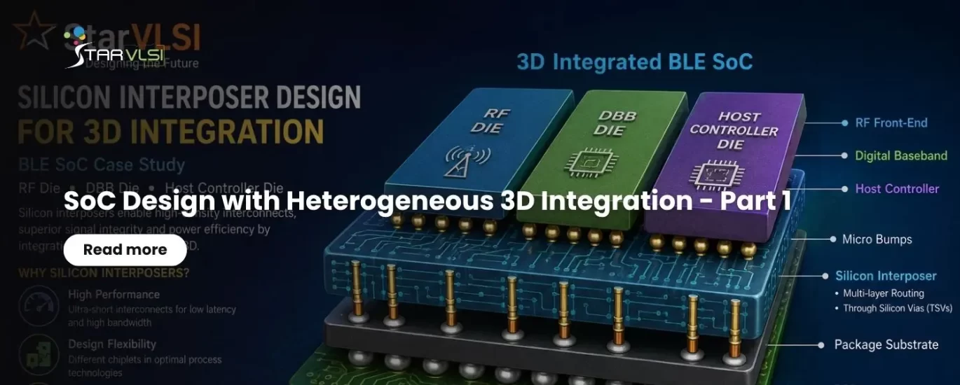
To understand the practical implementation of silicon interposer technology, consider a BLE SoC partitioned into three independently manufactured chiplets. The first die contains the complete RF front-end responsible for wireless transmission and reception. The second die implements the Digital Baseband responsible for packet processing and protocol execution. The third die integrates the Host Controller, processor subsystem, embedded memories, and peripheral interfaces.
The silicon interposer beneath these chiplets provides thousands of fine-pitch electrical connections that replace the long package traces used in conventional packaging technologies. Each chiplet communicates with the others through dedicated high-speed interfaces implemented using micro-bump arrays.
For example, digitized I/Q data generated by the RF front-end is transferred to the Digital Baseband through wide parallel buses implemented on the interposer. Similarly, decoded packet information is communicated from the Digital Baseband to the Host Controller over dedicated low-latency interfaces. Because these communication paths are only a few millimeters long, propagation delay and energy consumption are significantly lower than equivalent PCB-based interconnections.
This partitioning strategy also enables independent verification, testing, and replacement of individual chiplets during product development, substantially reducing design risk.
Through Silicon Vias (TSVs) in 3D Integration
Through Silicon Vias form the vertical electrical connections that enable communication through the thickness of the silicon interposer. These microscopic copper-filled cylindrical structures connect the upper routing layers to the package substrate beneath the interposer.
From a design perspective, TSV placement is one of the earliest architectural decisions because it affects routing congestion, power distribution, thermal conduction, and mechanical reliability. Although TSVs occupy relatively little silicon area individually, thousands of TSVs collectively consume significant routing resources and therefore require careful planning.
Power TSVs are generally distributed uniformly throughout the interposer to minimize voltage drop, while high-speed signal TSVs are strategically located near chiplet interfaces to reduce routing length. Ground TSVs often surround sensitive RF signal paths, creating electromagnetic shielding that reduces coupling between noisy digital signals and precision analog circuits.
The designer must also consider TSV keep-out zones because mechanical stress around each TSV can slightly alter transistor characteristics in nearby active silicon regions.
Floorplanning the BLE Chiplets on the Silicon Interposer
Unlike conventional floorplanning where all functional blocks are placed inside a single die, interposer floorplanning focuses on the relative placement of entire chiplets. This requires simultaneous optimization of electrical performance, thermal behavior, manufacturability, and package assembly.
In the BLE case study, the RF die should ideally be positioned near the antenna connection to minimize RF routing length and insertion loss. Since RF circuits are highly susceptible to digital switching noise, adequate separation from the Digital Baseband die is maintained. Ground shielding and dedicated analog power domains further improve isolation.
The Digital Baseband die acts as the communication hub between the RF subsystem and the Host Controller. Therefore, it is typically placed centrally on the interposer to minimize communication distance to both neighboring dies.
The Host Controller, containing processor cores and memories, is generally located near external interfaces such as USB, SPI, UART, or PCIe connections to reduce routing complexity toward package pins.
Good interposer floorplanning therefore minimizes latency while simultaneously reducing routing congestion, power loss, and thermal hotspots.
Interposer Routing Strategy
Once the chiplets have been placed on the silicon interposer, the next major task is designing the routing architecture that interconnects them. Unlike conventional PCB routing, where signal traces are measured in centimeters, silicon interposer routing occurs over distances of only a few millimeters using metal layers fabricated with semiconductor processing technology. This enables routing pitches of only a few micrometers, allowing thousands of high-speed signals to be carried simultaneously with excellent electrical characteristics.
For the BLE SoC considered in this case study, most traffic flows between the RF die and the Digital Baseband die. These include digitized I/Q samples, calibration parameters, Automatic Gain Control (AGC) information, PLL control signals, transmit gain settings, RSSI measurements, and synchronization information. The Digital Baseband then exchanges packet descriptors, encryption keys, DMA requests, interrupt signals, and control information with the Host Controller die.
To efficiently support these communication paths, the routing architecture is typically partitioned into dedicated regions. One region carries high-speed differential buses between the RF and Baseband dies, another handles processor interfaces between the Baseband and Host Controller, while separate routing channels are reserved for clocks, resets, power management signals, and debug interfaces. Sensitive RF control signals are isolated from noisy digital buses using grounded shielding tracks and guard routing.
Length matching becomes particularly important for wide parallel buses. Even though routing distances are short, timing skews between adjacent signals can degrade receiver timing margins at multi-gigabit data rates. Therefore, designers carefully balance the physical lengths of high-speed traces while minimizing vias and routing discontinuities.
Another practical consideration is routing scalability. Engineers often reserve unused routing resources for future product derivatives that may include additional chiplets such as embedded Flash memory, AI accelerators, sensor interfaces, or Ultra-Wideband (UWB) radios. Planning for future expansion during the first-generation interposer design significantly reduces redesign effort for subsequent products.
Designing an Efficient Power Delivery Network (PDN)
A silicon interposer not only routes signals but also acts as the primary power distribution backbone for all chiplets within the package. Every processor core, RF block, PLL, memory, and peripheral ultimately receives power through the interposer, making Power Delivery Network (PDN) design one of the most critical aspects of successful heterogeneous integration.
The BLE SoC considered in this example contains multiple voltage domains. The RF power amplifier operates from a relatively high supply to maximize transmission range, while the RF synthesizer, mixers, ADCs, DACs, and Low Noise Amplifier require extremely clean analog supplies with very low noise. The Digital Baseband typically operates at a low core voltage optimized for switching power, while the Host Controller may include independent voltage domains for processor cores, memories, I/O interfaces, and always-on logic.
These independent supplies must be distributed through dedicated TSV arrays and wide interposer metal layers capable of carrying high transient currents. Unlike conventional PCB power planes, the fine metal geometries inside the interposer require careful current density analysis to prevent electromigration and excessive IR drop.
Power TSVs are distributed uniformly beneath each chiplet, while ground TSVs surround analog circuitry to reduce return path impedance. Decoupling capacitors are strategically placed near each die to provide instantaneous current during switching events, reducing supply voltage fluctuations.
Modern interposer PDN design typically involves extensive Power Integrity (PI) simulations that evaluate IR drop, dynamic voltage noise, simultaneous switching noise, and resonance across the complete package. These simulations are performed long before tape-out to ensure stable operation under worst-case operating conditions.
Part 1 of 2 — StarVLSI Blog. Subscribe to get notified when Part 2 goes live.