Home › Blog › Best VLSI Training Institute in Bangalore
Best VLSI Training Institute in Bangalore: Courses, Fees, Placement & Career
- What Is a VLSI Course? A Quick Overview
- Why Bangalore Is India's VLSI Capital
- Top VLSI Training Institutes in Bangalore (2025)
- VLSI Training by Bangalore Location
- VLSI Course Syllabus: What You'll Learn
- VLSI Course Fees in Bangalore
- Career in VLSI: Roles, Salaries & Companies
- How to Choose the Right VLSI Institute
- FAQs
India's semiconductor industry is in the middle of a once-in-a-generation boom. With the government's ₹76,000 crore semiconductor incentive scheme attracting global chip giants, and companies like Micron, TATA Electronics, and CG Power setting up fabs, the demand for trained VLSI engineers has never been higher.
Bangalore — home to the chip design R&D centres of Intel, Qualcomm, Samsung, Synopsys, Cadence, and hundreds of VLSI service companies — sits at the epicentre of this transformation. If you are looking for a VLSI course in Bangalore that can genuinely launch your engineering career, this guide will help you make the right decision.
We cover everything: top VLSI training institutes in Bangalore, realistic fees, course duration, syllabus, placement track records, and a neighbourhood-by-neighbourhood breakdown for students across the city.
1. What Is a VLSI Course? A Quick Overview
VLSI (Very Large Scale Integration) is the engineering discipline behind the design of modern semiconductor chips — the processors in your phone, the AI accelerators in data centres, and the chips powering autonomous vehicles. A VLSI course teaches you how to go from a circuit concept to a manufacturable chip.
The VLSI design flow broadly splits into two domains:
- Frontend / RTL Design — Writing hardware description code (Verilog/VHDL), logic synthesis, simulation, and verification (including DFT, Formal Verification).
- Backend / Physical Design — Converting a netlist into a physical layout ready for the foundry: floorplanning, placement, clock tree synthesis (CTS), routing, signoff, and DRC/LVS checks.
A VLSI certification course from a credible institute bridges the gap between your degree knowledge and the highly specific, tool-driven skills that companies like Qualcomm, MediaTek, and Synopsys demand from day one.
Backend Physical Design is currently the most in-demand VLSI skill in Bangalore, with the widest fresher hiring window. Most openings at sub-7nm node companies specifically require hands-on EDA tool experience — something only specialised VLSI training institutes provide.
2. Why Bangalore Is India's VLSI Capital
Choosing VLSI training in Bangalore over any other city is not just about convenience — it is a strategic career advantage. Here's why:
- Chip design density: Bangalore hosts the India design centres of Intel, Qualcomm, Broadcom, Samsung Semiconductor, Arm, Renesas, NXP, and Analog Devices, among hundreds of others.
- VLSI services ecosystem: Companies like eInfochips, L&T Technology Services, Wipro VLSI, HCL Semiconductors, and countless boutique chip design houses are headquartered or heavily staffed in the city.
- EDA tool companies: Both Synopsys and Cadence — makers of the primary Physical Design tools (IC Compiler, Innovus) — have large Bangalore offices, meaning trainers with real industry depth are based here.
- Startup VLSI scene: Saankhya Labs, Mindgrove Technologies, and a growing wave of fabless startups are hiring trained freshers aggressively.
Simply put, getting your VLSI coaching in Bangalore puts you in the same city as your future employer — giving you a structural networking advantage from day one of your course.
3. Top VLSI Training Institutes in Bangalore (2025)
There are several VLSI design training institutes in Bangalore. We have evaluated them across five parameters: curriculum relevance, EDA tool access, faculty industry experience, placement support, and student outcomes.
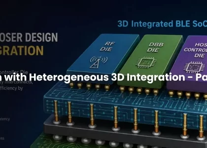
StarVLSI is a specialist VLSI training institute entirely focused on Backend Physical Design — the highest-demand, highest-paying track in VLSI today. Unlike generalist institutes that try to cover everything superficially, StarVLSI runs an intensive, project-driven program taught by working industry engineers with sub-7nm tape-out experience.
Students work on real EDA tools including Synopsys IC Compiler II and Cadence Innovus throughout the program — not just theory or PDFs. The curriculum mirrors what a junior Physical Design Engineer is expected to do on their first project.
- 100% Backend PD focus
- Industry mentor faculty
- Real EDA tool access
- Project-based learning
- Placement support
- Small batch sizes
Maven Silicon is one of the larger VLSI training institutes in Bangalore with multiple tracks covering both frontend (RTL, Verification) and backend flows. Good for students who want broad exposure across the VLSI spectrum before specialising.
- Multiple specialisations
- Large alumni network
- Online + offline batches
Cranes Varsity is a long-standing engineering training institute with VLSI as one of many offerings. Best suited for students who want VLSI training alongside other engineering skill programs. Their VLSI-specific depth is moderate compared to specialist institutes.
- Established institution
- Multiple domains
- Physical classrooms
Chipxpert is a focused VLSI institute with a reasonable track record in RTL design and synthesis training. Placement outcomes vary based on batch — it is worth speaking to alumni before enrolling.
- VLSI-focused curriculum
- Certification support
These institutes are growing players in the Bangalore VLSI training space. Both offer basic-to-intermediate VLSI curriculum. Verify tool access and faculty credentials carefully before deciding.
- Competitive fees
- Smaller class sizes
Always ask prospective institutes: (1) Do students get hands-on EDA tool access, or just demos? (2) What percentage of recent batch graduates are placed, and at which companies? (3) Who teaches the course — full-time academics or working industry professionals? These three questions will reveal more than any brochure.
Quick Comparison: Top VLSI Institutes in Bangalore
| Institute | Specialisation | EDA Tools | Placement Support | Best For |
|---|---|---|---|---|
| StarVLSI | Backend Physical Design | IC Compiler II, Innovus | Dedicated | PD career starters |
| Maven Silicon | Frontend + Backend | Moderate access | Moderate | Broad exposure |
| Cranes Varsity | General Engineering | Limited | General | Multi-domain students |
| Chipxpert | VLSI / RTL | Moderate | Variable | RTL / DV learners |
| VLSI First | Beginner VLSI | Basic | Limited | Introductory learners |
4. VLSI Training by Bangalore Location
Bangalore's tech clusters are spread across the city — and so are the students searching for VLSI training near me. Here's a location guide to help you find the right program from your neighbourhood.
| Area | Nearest VLSI Hub | Commute Note |
|---|---|---|
| Marathahalli | Directly in tech corridor | Excellent Access |
| Whitefield | ITPL / Outer Ring Road cluster | Excellent Access |
| HSR Layout | Sarjapur Road corridor | Very Close |
| Koramangala | Central tech zone | Very Close |
| BTM Layout | Close to Silk Board hub | Moderate |
| Electronic City | Infosys, HCL, Wipro campus zone | Excellent Access |
| Indiranagar | Central + metro-connected | Moderate |
| Jayanagar | South Bangalore residential | Moderate |
| Rajajinagar | West Bangalore, metro link | Moderate |
StarVLSI accepts students from across Bangalore regardless of area. Most students from Marathahalli, HSR Layout, Whitefield, Koramangala, and Electronic City find the commute very manageable. Contact the team at +91 89514 18316 to confirm the current training centre location closest to you.
5. VLSI Course Syllabus: What You'll Learn
A quality VLSI design course should cover both theoretical fundamentals and hands-on EDA tool workflows. Below is the structured syllabus for StarVLSI's Backend Physical Design program — one of the most comprehensive in Bangalore.
- Digital electronics refresher
- MOS transistor theory
- CMOS logic gates & timing
- VLSI design flow overview
- Verilog HDL basics
- Logic synthesis with Design Compiler
- SDC constraints writing
- Synthesis reports & analysis
- Die area estimation
- Macro placement strategies
- Power planning & IR drop
- IO pad placement guidelines
- Global & detailed placement
- Congestion analysis
- Timing-driven placement
- Scan chain reordering
- Clock topology planning
- CTS implementation (IC Compiler II)
- Skew & latency analysis
- Multi-clock domain handling
- Global & detailed routing
- DRC / LVS checks
- Static Timing Analysis (STA)
- IR drop & EM signoff
Synopsys IC Compiler II · Cadence Innovus · Synopsys Design Compiler · PrimeTime STA · StarRC · Calibre DRC/LVS — the same tools used in industry at Qualcomm, Intel, and MediaTek.
6. VLSI Course Fees in Bangalore: What to Expect
One of the most common questions from prospective students is: "What is the VLSI training fee in Bangalore?" Here is an honest breakdown across the market.
| Course Type | Typical Fee Range | Duration | Tool Access |
|---|---|---|---|
| Basic VLSI (beginner) | ₹25,000 – ₹45,000 | 2–3 months | Limited / demo |
| RTL / DV Specialist | ₹45,000 – ₹75,000 | 3–4 months | Moderate |
| Backend Physical Design (StarVLSI) | Contact for pricing | 4–5 months | Full EDA access |
| ASIC Design Full Stack | ₹80,000 – ₹1,20,000 | 5–6 months | Comprehensive |
Pro tip on fees: Do not choose a VLSI institute based on the lowest fee. The key ROI metric is not what you pay — it is what you earn within 6 months of completing the course. A ₹10,000 cheaper course that doesn't get you hired costs infinitely more than a premium program with a strong placement track record.
For current StarVLSI fees and batch dates, speak directly with the admissions team at +91 89514 18316 or email info@starvlsi.com.
7. Career in VLSI: Roles, Salaries & Hiring Companies
A question candidates often ask: "Is VLSI a good career in 2025?" The short answer is yes — and the numbers back it up. Here's the hiring landscape for trained VLSI engineers in Bangalore and across India.
VLSI vs Embedded Systems: Which Should You Choose?
A common dilemma for ECE/EEE graduates. Here's a direct comparison:
| Parameter | VLSI / Chip Design | Embedded Systems |
|---|---|---|
| Entry barrier | Higher (specialised tools) | Moderate |
| Fresher salary | ₹6 – 18 LPA | ₹3.5 – 8 LPA |
| Job volume | Growing fast (India Semi mission) | Large but competitive |
| Key companies | Qualcomm, Intel, MediaTek | Bosch, Continental, TCS |
| Skillset | EDA tools, HDL, timing | C/C++, RTOS, protocols |
If you have an ECE/EEE background and can invest 4–5 months in specialised training, VLSI career potential significantly outpaces embedded systems at the fresher level — especially in Bangalore.
8. How to Choose the Right VLSI Training Institute in Bangalore
The market for VLSI coaching in Bangalore has grown rapidly, which means quality varies widely. Here is a practical checklist to protect your investment:
- Verify EDA tool access: Ask if students get dedicated seat access to industry-standard tools (IC Compiler II, Innovus, PrimeTime) — not just instructor demos.
- Ask about faculty background: Confirm instructors have actual tape-out or silicon experience at recognised companies, not just academic VLSI knowledge.
- Request recent placement data: Ask for the last 2–3 batches' placement rate and the names of hiring companies. Be sceptical of vague claims.
- Evaluate curriculum depth: A good backend PD course must cover DRC/LVS signoff, STA, and multi-mode multi-corner (MMMC) analysis — not just placement and routing basics.
- Check batch size: Large batches (30+) compromise hands-on time per student. Smaller batches mean more tool time and mentor interaction.
- Talk to alumni: Ask the institute to connect you with recent graduates. A confident institute will have no hesitation doing this.
- Assess post-training support: Does the institute provide mock interviews, resume help, and referrals to hiring companies? Or does the support end on the last day of class?
While everyone competes on "VLSI training Bangalore," the real demand is shifting to "VLSI placement training Bangalore", "VLSI course with real projects", and "VLSI job guarantee Bangalore". When evaluating institutes, ask specifically about their placement process — not just their course content.
Why StarVLSI Stands Apart for Backend Physical Design
- 100% specialisation: StarVLSI does one thing — Backend Physical Design — and does it at the depth that industry demands. No diluted multi-domain curriculum.
- Industry instructors: Every session is led by engineers with real tape-out experience, not theoretical trainers.
- Real EDA tools from Day 1: Students work on the same tools (IC Compiler II, Innovus) used in production at Qualcomm and MediaTek.
- Project-based assessment: Graduates complete a full Physical Design project they can demonstrate in interviews — a significant competitive advantage.
- Placement-linked curriculum: The course content is continuously updated based on what Bangalore's hiring companies are actually testing in technical interviews.
9. Frequently Asked Questions
VLSI training fees in Bangalore range from ₹25,000 for basic introductory programs to ₹1,20,000 for comprehensive multi-specialisation courses. Specialist programs like StarVLSI's Backend Physical Design course are priced competitively and offer strong ROI through placement outcomes. Contact +91 89514 18316 for current pricing.
Most VLSI design courses run between 3 to 6 months. StarVLSI's Backend Physical Design program is structured as a 4–5 month intensive, with timing designed to align with industry hiring cycles — particularly for Q1 and Q3 recruitment drives.
Some institutes offer online VLSI training. However, for Backend Physical Design specifically, hands-on EDA tool access is non-negotiable — something that remote setups struggle to deliver effectively. StarVLSI offers classroom-based training to ensure full tool access and mentorship quality. Online batches may be considered — contact the team for the latest format options.
Most reputable VLSI training institutes require a B.E. / B.Tech in ECE, EEE, or Electronics. Some programs also accept M.Tech students and working engineers looking to switch into chip design. Foundational knowledge of digital electronics is strongly recommended before enrolling in a specialised VLSI course.
Freshers with quality VLSI training are hired as Physical Design Engineers, RTL Design Engineers, VLSI Verification Engineers, and DFT Engineers. Salary packages range from ₹6 LPA to ₹18 LPA depending on specialisation, company, and project complexity. Companies hiring VLSI freshers in Bangalore include Qualcomm, MediaTek, Samsung, Synopsys, HCL Semiconductors, L&T Tech, and many startups.
Yes. StarVLSI is accessible to students from Marathahalli, Koramangala, HSR Layout, Whitefield, BTM Layout, and Electronic City. Contact the admissions team to confirm the current training location and the best commute route from your area.
For ECE/EEE graduates in Bangalore, VLSI offers higher fresher salaries, faster career growth, and exposure to global chip design companies. The entry barrier is higher and requires specialised training — but the returns are substantially better for those who invest in quality VLSI coaching.
Ready to Start Your VLSI Career?
StarVLSI's next Backend Physical Design batch is forming now. Seats are limited to ensure hands-on EDA tool time for every student.
📞 +91 89514 18316 | +91 81238 88866 | ✉️ info@starvlsi.com