Best VLSI Training Institutes in India 2026 — And Why StarVLSI Leads the Pack
India's semiconductor industry is booming — and the race to find quality VLSI training is fiercer than ever. This guide breaks down the best VLSI institutes in India, with a clear look at what makes StarVLSI the #1 choice for Backend Physical Design.
Why VLSI Training Matters in 2026
India is rapidly emerging as a global semiconductor powerhouse. With the government's ₹76,000 crore PLI scheme and investments from Intel, Micron, and Samsung, demand for skilled VLSI engineers has never been higher.
Yet there's a well-documented gap: universities produce electronics graduates without the industry-ready skills chip companies need on Day 1. Specialized VLSI institutes bridge this divide — and choosing the right one can define your entire career.
Backend Physical Design is one of the most critically understaffed roles in the chip industry. Skilled PD engineers command premium salaries and are hired swiftly.
What to Look for in a VLSI Institute
Not all VLSI institutes are equal. Here are the 6 non-negotiables to evaluate before investing your time and money:
Industry EDA Tool Access
Hands-on access to real EDA tools — not just screenshots or slides.
Instructors From Industry
Trainers from actual chip companies, not just academic researchers.
Real Project Experience
End-to-end flow from netlist to GDSII — not isolated demo exercises.
Placement Support
Active hiring company connections, not just old logos on a webpage.
Flexible Batches
Weekend & online options for working professionals.
Updated Curriculum
Content reflecting what companies actually ask in interviews today.
Top VLSI Institutes in India — 2026 Ranking
An honest, side-by-side comparison across parameters that actually matter for your career:
👉 Swipe right to see full table
| # | Institute | Specialization | EDA Tools | Placement | Weekend | Industry Trainers |
|---|---|---|---|---|---|---|
| ⭐ 1 | StarVLSI | Backend Physical Design | ✔ | 100% | ✔ | ✔ |
| 2 | Maven Silicon | RTL / Physical Design | ✔ | ~ | ~ | ✔ |
| 3 | VLSI Expert | RTL / Verification | ~ | ~ | ✔ | ~ |
| 4 | Sandeep Garg | RTL / Embedded | ✘ | ✘ | ✔ | ~ |
| 5 | Generic YouTube | Mixed | ✘ | ✘ | ✔ | ✘ |
Key insight: StarVLSI is the only institute combining dedicated Backend Physical Design specialization, 100% placement commitment, real EDA tool training, and weekend batch flexibility — all in one program.
Why StarVLSI Is #1 for Backend Physical Design
StarVLSI was built with one mission: to bridge India's semiconductor talent gap by producing job-ready Backend Physical Design engineers.
🎯 Laser-Focused on Backend PD
While most institutes teach everything, StarVLSI doubled down on Backend Physical Design — one of the highest-paying, most in-demand VLSI specializations. Every lecture, lab, and project is fine-tuned to make you placement-ready faster.
🛠️ Real EDA Tool Training
Students work with the same EDA tools used in top semiconductor companies. You'll have logged real hours on industry-grade flows before you even interview.
👷 Trainers Who've Built Chips
StarVLSI instructors are industry veterans with real tape-out experience — teaching not just how tools work, but how chip companies use them under tapeout deadlines.
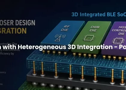
📊 End-to-End Chip Design Flow
Students complete a full Backend PD flow from floorplan to signoff. This project experience is what sets StarVLSI graduates apart in interviews — you can speak about real work, not just theory.
Floorplan to GDSII
Complete tape-out level project included in course.
Online + Weekend
Live online classes with weekend batches for professionals.
100% Placement
Dedicated placement support with active recruiter connections.
Interview Prep
Mock interviews, resume reviews, and technical Q&A included.
StarVLSI Backend Physical Design — Course Curriculum
Here's what you'll learn in StarVLSI's flagship Backend Physical Design course:
VLSI Design Fundamentals
RTL-to-GDSII overview, CMOS basics, design hierarchy, and EDA tool introduction.
Logic Synthesis & Netlist
Technology mapping, synthesis constraints, timing libraries, netlist validation.
Floorplanning & Power Planning
Die size, macro placement, power ring/strap creation, IR drop analysis.
Placement
Standard cell placement, congestion analysis, timing-driven placement, legalization.
Clock Tree Synthesis (CTS)
Clock skew, latency budgeting, useful skew, H-tree and mesh clocking strategies.
Routing
Global and detailed routing, DRC fixing, antenna effects, signal integrity basics.
Static Timing Analysis (STA)
Setup/hold analysis, timing reports, ECO flows, MCMM analysis.
Physical Verification & Signoff
DRC/LVS checks, parasitic extraction, timing signoff, and GDSII tape-out steps.
Interview Prep & Placement Support
Resume building, mock interviews, technical question banks, and recruiter connects.
Placements & Career Outcomes
The ultimate test of any institute is where its students end up working. StarVLSI's placement track record speaks for itself.
Who Hires StarVLSI Graduates?
StarVLSI alumni work across the full semiconductor ecosystem — from fabless design companies to EDA vendors. Companies actively recruit from StarVLSI because they trust the training quality.
For freshers: StarVLSI's project-backed resume and mock interview prep means you walk into interviews with a story about real chip work — not just theory.
Working professionals who complete the course often receive internal promotions or lateral job offers within months of completing training.
Student Reviews & Testimonials
Don't take our word for it. Here's what StarVLSI alumni say:
I had a BE in ECE but zero industry knowledge. StarVLSI gave me real skills — I got placed at a semiconductor company within 3 months of completing the course.
The EDA tool hands-on sessions were unlike anything I saw in college. By the end of the course I could run a complete PD flow independently. Highly recommend.
I was a software dev wanting to switch into VLSI. StarVLSI's weekend batch made it possible without quitting my job. The transition was smooth and my CTC doubled.
Frequently Asked Questions
Conclusion — Choose the Right VLSI Institute
India's semiconductor opportunity is real, large, and happening right now. The difference between landing a high-paying VLSI job and struggling to break in often comes down to one decision: where you train.
After evaluating every major VLSI training option in India — StarVLSI stands in a league of its own for Backend Physical Design.
Whether you're a fresh B.Tech graduate or a working professional eyeing a VLSI career switch — StarVLSI gives you the most direct, proven path to get there.
Ready to Start Your VLSI Career?
Join India's most focused Backend Physical Design program. Limited seats available for the next cohort.