IC Packages and Package Selection for Mixed-Signal SoCs
IC packaging has grown from a simple protective enclosure into a critical driver of electrical, thermal, and mechanical performance. This article walks through the major IC package technologies — from DIP to 2.5D/3D integration — the criteria for selecting the right package, and the specific design considerations for mixed-signal SoCs that combine analog, RF, low-frequency, and high-speed interfaces on one chip.
Importance of IC Packaging in System Design
Modern semiconductor devices are no longer evaluated solely by transistor density or silicon performance. As process technologies continue to shrink below 5 nm and heterogeneous integration becomes mainstream, IC packaging has become one of the most critical contributors to the overall performance, reliability, power efficiency, and manufacturability of a System-on-Chip (SoC). The package is no longer just a protective enclosure surrounding the silicon die — it has evolved into an essential part of the electrical, thermal, and mechanical design of the complete system.
Today's SoCs integrate diverse functional blocks such as high-performance processors, analog front ends, RF transceivers, memories, power management units, sensors, and multi-gigabit communication interfaces on a single chip. Each of these subsystems imposes unique requirements on package design. High-speed interfaces demand excellent signal integrity, RF blocks require low parasitic inductance and controlled impedance, analog circuits require low-noise environments, and power-intensive digital logic requires efficient thermal dissipation and robust power delivery. Consequently, selecting the right IC package has become an engineering decision that directly affects product performance and reliability.
Historically, IC packages primarily served as mechanical carriers that protected fragile silicon dies from environmental damage while providing electrical connections to printed circuit boards. As integrated circuits became increasingly complex, packaging technology had to evolve to address electrical performance, thermal management, miniaturization, and system integration challenges.
Modern package engineering is now tightly coupled with chip architecture and PCB design. The package influences power integrity, signal integrity, electromagnetic interference, clock distribution, thermal performance, manufacturing yield, and long-term reliability. In many advanced SoCs, package design begins simultaneously with chip floorplanning, allowing designers to optimize die layout, bump placement, substrate routing, and PCB escape routing together. This co-design methodology ensures that package parasitics and thermal effects are considered early in the design cycle rather than being treated as post-layout issues.
Different Types of IC Packages
The semiconductor industry offers a wide variety of package technologies, each optimized for different performance, cost, and manufacturing requirements. The selection depends on factors such as pin count, operating frequency, thermal dissipation, package size, production volume, and application domain.
| Package | Key Trait | Typical Applications |
|---|---|---|
| DIP Dual In-Line Package |
Through-hole, mechanically robust, but high lead parasitics | Educational kits, lab equipment, industrial control |
| QFP Quad Flat Package |
Leaded, pins on all four sides, several hundred I/Os | Automotive MCUs, industrial processors, DSPs |
| QFN Quad Flat No-Lead |
Leadless, exposed thermal pad, low inductance | BLE, Wi-Fi, sensor ICs, PMICs, mixed-signal ASICs |
| BGA Ball Grid Array |
Solder-ball array under package, high I/O density | Processors, networking ASICs, FPGAs, automotive SoCs |
| FCBGA Flip-Chip BGA |
Die flipped & bump-connected, shortest signal paths | CPUs, GPUs, AI processors, networking switches |
| WLCSP Wafer-Level Chip Scale |
Bumps formed pre-dicing, package ≈ die size | Smartphones, wearables, MEMS, compact IoT |
| FOWLP Fan-Out Wafer-Level |
I/O redistributed beyond die edge, low parasitics | Mobile processors, RF front-end modules, radar |
| SiP System-in-Package |
Multiple dies in one module, heterogeneous integration | Wearables, IoT, medical devices, automotive sensors |
| 2.5D / 3D Interposer & TSV Stacking |
Ultra-short interconnects, very high bandwidth | AI accelerators, HPC, networking, domain controllers |
Dual In-Line Package (DIP)
The Dual In-Line Package was one of the earliest IC package technologies and remains familiar to every electronics engineer. With two parallel rows of through-hole pins, DIP packages provide excellent mechanical robustness and are easy to assemble manually. Although they are still widely used in educational kits, laboratory equipment, and certain industrial control applications, they are no longer suitable for modern high-performance SoCs. Their long leads introduce significant parasitic inductance and capacitance, making them unsuitable for high-speed digital or RF applications where signal integrity is critical.
Quad Flat Package (QFP)
The Quad Flat Package became popular as integrated circuits required larger pin counts without dramatically increasing package size. QFP packages distribute pins along all four sides of the package, allowing several hundred I/O connections while maintaining relatively simple PCB assembly.
QFP remains widely used for automotive microcontrollers, industrial processors, communication controllers, and digital signal processors. However, as clock frequencies increase into the multi-gigahertz range, the lead inductance associated with external pins begins to limit electrical performance, encouraging designers to migrate toward leadless package technologies.
Quad Flat No-Lead (QFN)
QFN packages represent a significant improvement over conventional leaded packages by eliminating protruding leads altogether. Electrical connections are provided through exposed metal pads located underneath the package, dramatically reducing lead inductance while improving thermal conductivity.
This package technology has become extremely popular for Bluetooth devices, Wi-Fi chipsets, sensor interfaces, power management ICs, and mixed-signal ASICs because it offers excellent RF characteristics, compact size, and low manufacturing cost. The exposed thermal pad beneath the package also provides an efficient path for dissipating heat into the PCB.
Ball Grid Array (BGA)
As processor complexity increased, conventional perimeter-lead packages could no longer support the required number of input/output connections. Ball Grid Array technology addressed this challenge by replacing peripheral leads with an array of solder balls distributed across the entire underside of the package.
The shorter electrical paths offered by BGA significantly reduce parasitic inductance while improving power delivery and thermal performance. Modern processors, networking ASICs, FPGAs, AI accelerators, and automotive SoCs commonly employ BGA packages because they provide high I/O density and excellent electrical characteristics suitable for multi-gigabit communication interfaces.
Flip-Chip Ball Grid Array (FCBGA)
Flip-chip packaging represents one of the most important advances in semiconductor packaging. Instead of wire bonding the silicon die to the package substrate, the die is flipped upside down and connected directly using microscopic solder bumps.
This direct electrical connection dramatically reduces signal path length, minimizes parasitic inductance, and improves both power integrity and thermal dissipation. Because heat can flow directly from the backside of the silicon to a heat spreader, flip-chip packages support significantly higher power densities than conventional wire-bond packages. Consequently, virtually all modern CPUs, GPUs, AI processors, networking switches, and advanced automotive processors utilize flip-chip packaging.
Wafer-Level Chip Scale Package (WLCSP)
Wafer-Level Chip Scale Packaging eliminates much of the conventional package structure by creating solder bumps directly on the silicon wafer. Since packaging occurs before wafer dicing, the resulting package is almost identical in size to the silicon die itself.
The extremely compact dimensions, excellent electrical performance, and low manufacturing cost make WLCSP highly attractive for smartphones, wearable electronics, MEMS sensors, Bluetooth devices, and compact IoT products where board area is a premium.
Fan-Out Wafer-Level Packaging (FOWLP)
Fan-Out packaging extends wafer-level packaging by redistributing I/O connections beyond the physical dimensions of the silicon die. This enables significantly higher pin counts without increasing silicon size.
Because fan-out packages exhibit very low electrical parasitics and excellent thermal characteristics, they are widely used in high-performance mobile processors, RF front-end modules, automotive radar devices, and advanced communication chipsets.
System-in-Package (SiP)
Rather than integrating every function onto a single silicon die, System-in-Package technology assembles multiple dies within a common package. A typical SiP may combine processors, memory, RF transceivers, analog front ends, passive components, and power management ICs into one compact module.
This heterogeneous integration approach enables designers to optimize each die independently while reducing PCB area and improving overall system performance. SiP technology is increasingly popular in wearable electronics, IoT devices, medical equipment, and automotive sensor modules.
2.5D and 3D Advanced Packaging
Advanced computing applications have driven the adoption of 2.5D and 3D integration technologies. In 2.5D packaging, multiple silicon dies are mounted on a high-density silicon interposer that provides thousands of extremely short interconnections between chips. This approach enables very high memory bandwidth while reducing power consumption and latency.
Three-dimensional packaging extends this concept further by stacking dies vertically using Through-Silicon Vias (TSVs). Vertical integration dramatically shortens interconnect lengths, enabling extremely high bandwidth and compact form factors. These technologies are becoming indispensable for AI accelerators, high-performance computing systems, networking processors, and next-generation automotive domain controllers.
Selecting the Appropriate Package for a Mixed-Signal SoC
Selecting the optimum package involves balancing electrical performance, thermal efficiency, mechanical reliability, manufacturing cost, and future scalability. The package must support the required I/O count while minimizing parasitic inductance, resistance, and capacitance. At the same time, it must provide sufficient thermal conductivity to dissipate heat generated by increasingly power-dense SoCs.
Cost considerations are equally important. While advanced packages such as Flip-Chip BGA, Fan-Out, or 2.5D integration provide superior electrical performance, they also introduce greater manufacturing complexity and higher assembly costs. Consumer electronics may prioritize compact size and cost, whereas automotive and networking applications typically prioritize reliability and long-term performance.
The final selection therefore depends upon the application's operating frequency, environmental conditions, expected lifetime, production volume, thermal budget, and overall system architecture.
Package Design Considerations for Mixed-Signal Interfaces
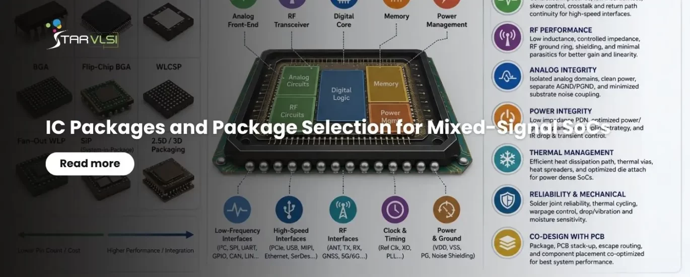
A mixed-signal SoC combines several fundamentally different electrical disciplines on one package, each with its own design priorities:
Thermal Management in Modern SoC Packages
As computational performance continues to increase, thermal management has become one of the most challenging aspects of package engineering. High-performance processors, AI accelerators, networking ASICs, and automotive SoCs routinely dissipate tens of watts of power within relatively small silicon areas.
Modern package designs therefore incorporate exposed thermal pads, copper heat spreaders, vapor chambers, thermal interface materials, and optimized heat sink attachment mechanisms to efficiently remove heat from the silicon. Thermal simulations performed during package development identify potential hot spots and ensure that junction temperatures remain within safe operating limits throughout the product lifetime.
Power Delivery and Signal Integrity Considerations
The package forms an integral part of the overall power delivery network between the PCB and the silicon die. Poor package design can introduce excessive voltage drop, simultaneous switching noise, and ground bounce, leading to timing failures and degraded analog performance.
Engineers therefore optimize package power and ground planes, strategically position decoupling capacitors, and perform comprehensive power integrity simulations to minimize voltage ripple. At the same time, signal integrity analysis evaluates insertion loss, crosstalk, impedance discontinuities, and package resonance to ensure reliable operation of high-speed communication interfaces.
Package–PCB Co-Design
Modern semiconductor development increasingly relies on package and PCB co-design methodologies. Rather than designing the silicon, package, and PCB independently, engineers optimize these elements simultaneously to achieve the best overall electrical and thermal performance.
This integrated design approach enables early identification of routing congestion, impedance mismatches, thermal bottlenecks, and power delivery challenges, thereby reducing costly design iterations and improving first-pass silicon success.
Conclusion
IC packaging has evolved from a simple protective enclosure into one of the most critical components of modern semiconductor system design. The selection of an appropriate package directly influences electrical performance, thermal efficiency, manufacturability, reliability, and overall system cost. For mixed-signal SoCs integrating analog circuitry, RF transceivers, low-frequency peripherals, and multi-gigabit communication interfaces, package design requires careful consideration of signal integrity, power delivery, thermal management, electromagnetic compatibility, and mechanical robustness.
As semiconductor systems continue toward heterogeneous integration and chiplet-based architectures, package engineering will become even more tightly coupled with silicon design and PCB development. For aspiring VLSI engineers, understanding IC packaging is no longer optional — it is an essential skill that bridges device-level design with system-level implementation. Mastery of modern packaging technologies will enable engineers to design reliable, high-performance, and scalable SoCs for automotive, industrial, AI, networking, and next-generation IoT applications, making packaging one of the defining technologies of the future semiconductor industry.
Master IC Packaging with StarVLSI
Build hands-on expertise in advanced packaging, mixed-signal design, and modern EDA tools to prepare for the next generation of heterogeneous SoC development.
Explore StarVLSI CoursesStay connected with the StarVLSI Blog for more in-depth articles on advanced VLSI design, semiconductor packaging, RF systems, physical design, verification methodologies, and emerging technologies shaping the future of the semiconductor industry.