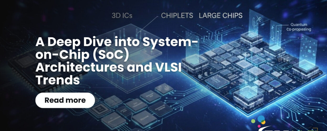
SoC architecture lies at the heart of today’s hyper-connected digital world, powering smartphones, wearables, automotive systems, servers, and cloud infrastructure. Chapter 1 of SoC Physical Design: A Comprehensive Guide explains how modern System-on-Chip designs have evolved from discrete components into highly integrated compute platforms. This article breaks down the engineering principles of SoC architecture and highlights the key semiconductor and VLSI trends shaping the future—aligned with StarVLSI’s mission of developing industry-ready chip design talent.
System-on-Chip (SoC)
A System-on-Chip (SoC) integrates almost all functions of an electronic system, computation, communication, control, data storage, power management, sensing, and user interface onto a single piece of silicon. According to Chapter 1, SoC processes analog and digital inputs, stores data, performs computation, and drives output signals to control other systems, all while occupying minimal real estate on the wafer.
Because CMOS (Complementary Metal-Oxide-Semiconductor) technology continues to scale into nanometer regimes, SoCs today contain hundreds of functional blocks, processor cores, memories, accelerators, peripheral interfaces, and analog front-ends.
Trends Shaping SoC Evolution
The chapter highlights multiple key trends in reshaping SoC architecture. Let’s unpack them.
1. Continued CMOS Scaling with Advanced Lithography
Moore’s Law may be slowing, but scaling has not stopped.
Chapter 1 (page 2) explains how EUV (Extreme Ultraviolet) lithography, multi-patterning, and FinFET/GAA architectures push feature sizes below 3 nm, enabling denser and more complex SoCs.
2. The Impact of Dennard Scaling Slowdown
Dennard scaling predicted that as transistors shrink, power density remains constant.
However, below 5 nm, the chapter notes diminishing performance benefits—triggering:
- new device structures
- innovative integration techniques
- smarter EDA (Electronic Design Automation) platforms
3. Heterogeneous Integration Becomes the Norm
- SoCs of today combine:
- digital cores
- analog/mixed-signal blocks
- RF transceivers
- on-chip sensors
- dense memories
- specialized AI engines
This allows each functional block to be realized in the most optimal technology.
4. Rise of Magnetic RAM and Non-Volatile Memory
The book highlights new memory technologies such as STT-MRAM, SOT-MRAM, and VCMA-MRAM (page 4), likely to complement or replace SRAM caches in future designs.
5. Edge AI and Real-Time Inference
With 5G, smart wearables, AR/VR, and autonomous systems, SoCs must perform AI inference on the edge—not in the cloud.
The chapter states that analog compute-in-memory and domain-specific accelerators are key emerging directions.
6. Wafer-Scale SoCs
The Cerebras wafer-scale AI chip is highlighted as an example of going “beyond chips to entire wafers” for extreme compute workloads.
7. Scalable Multi-Core CPU Fabrics
Cloud/datacenter systems demand horizontally scalable architectures—breaking compute, memory, and I/O into modular partitions.
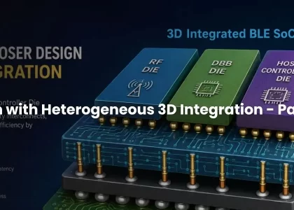
8. 3D-IC and Chiplet Architectures
Chiplets stacked vertically using TSVs (Through-Silicon Vias) or silicon interposers form hybrid systems with unmatched flexibility.
Chapter 1 explains that heterogeneous chiplets bring RF, memory, compute, and sensors together efficiently.
The Building Blocks of SOC
The book divides an SoC into key categories:
1. Analog Blocks
Analog front ends, ADC/DACs, PLLs, LDOs, RF transceivers—designed using full-custom techniques due to their sensitivity to noise and precision requirements.
2. Digital Cores
These include synthesizable processors, accelerators, security engines, and communication stacks, implemented as soft IP (RTL) or hard IP (GDS).
3. Embedded Memory Blocks
SRAM, ROM, OTP, FLASH, and compiler-generated memories, often supporting BISR/BISA (Built-In Self-Repair / Self-Analysis).
4. Macros – Hard and Soft
Reusable sub-systems packaged as IP that integrate seamlessly into larger SoCs.
Design Abstraction – From Idea to Silicon
Chapter 1 of the book clearly outlines the abstraction hierarchy of SoC design :
- SystemC / SystemVerilog Models – functional architecture
- RTL (Register Transfer Level)
- Gate-Level Netlists
- GDSII Layout – final physical mask-level representation
Soft macros can be modified; hard macros are fixed.
This modularity allows modern SoCs to scale to hundreds of IP cores.
SoC Design Methodology: Specification to Tape-Out
The chapter also presents a typical SoC design flow, starting from:
Specification → HDL Modeling → Verification → Synthesis → DFT → Floorplanning → PnR → Signoff → Tapeout. The chapter emphasizes the need for future SoC methodologies to evolve into hyper-convergent flows, especially with 3D-ICs and chiplet ecosystems.
SoC Design Styles: Custom, Semi-Custom, and Standard-Cell
The chapter categorizes design styles (pages 10–11):
- Custom Design Style
The design flow is used for:
- high-performance processors
- analog/RF blocks
- specialized circuits
- Semi-Custom Design Style
Gate Arrays and Structured ASICs.
- Standard Cell Design
The most widely used SoC design approach—achieving strong PPA (Performance, Power, Area) with the help of PDKs (Process Design Kits).
The Physical Design of SoCs
The chapter sets the stage for the remainder of the book by defining PD fundamentals—stick diagrams, re-convergent design models, file formats, PDKs, and EDA tools.
These lay the foundation for floorplanning, placement, CTS (Clock Tree Synthesis), routing, DFM (Design for Manufacturability), STA (Static Timing Analysis), and signoff flows discussed in later chapters.
Future Trends in SoC Designs
From the IRDS (International Roadmap of Devices and Systems), the chapter highlights:
- Feature scaling will plateau around 7–8 nm.
- Beyond-CMOS devices will emerge.
- AI will drive architectures that exceed human perception (e.g., vision systems).
- Quantum computing and stacked memories will shift compute paradigms.
- ML-enabled EDA tools will become mandatory for addressing design complexity.
In essence, the SoC of the future will be intelligent, heterogeneous, 3D-stacked, and application-driven.
Chapter 1 of SoC Physical Design – A Comprehensive Guide lays the perfect foundation for understanding what makes modern SoC design so powerful, so complex, and so essential.
It captures the full spectrum—from device physics and scaling limits to architecture, abstraction, and the future of semiconductor systems.
If you are aiming to stay relevant in the fast-evolving SoC industry, mastering these fundamentals is non-negotiable.
Stay Ahead with StarVLSI
Follow us on socials