
Physical Design is the most transformative phase in the chip development lifecycle. This is where abstract hardware descriptions, written in HDL (Hardware Description Language) are methodically shaped into geometric patterns that can be manufactured on silicon wafers.
Chapter 2 of SoC Physical Design – A Comprehensive Guide provides a structured, end-to-end view of this journey, explaining how SoC designers take the output of synthesis and convert it into a layout that satisfies timing, power, area, and manufacturability requirements.
This StarVLSI blog reinterprets this Chapter into a flowing, real-world narrative that new engineers and industry aspirants can understand and apply.
1. Understanding What SoC Physical Design Really Means
Physical Design begins after logic synthesis produces a gate-level netlist. This netlist is not yet a chip, it is simply a connectivity map showing which logic gates and macros should connect to each other. The Physical Design flow converts this netlist into a full-chip layout, complete with device placements and routed interconnects.
There are two types of netlists: flat and hierarchical netlists. Flat netlists place all logic elements on one level, making the design flow straightforward but unwieldy for large SoCs. Hierarchical netlists divide the design into blocks across multiple layers of hierarchy, making the design scalable and enabling teams to work on different parts in parallel.
2. Core and IO Design – The Two Worlds Within a Chip
Every SoC layout has two physical regions: the core area and the IO area. The core area houses the heart of the design: standard cells, memory, processors, accelerators, and analog blocks. The IO area surrounds this core and contains IO pads, power pads, ground pads, and ESD protection structures. The IO ring forms the interface between silicon and the package pins.
Power distribution also begins here. Multiple supply rails, core, IO, analog, memory, and others are routed through rings and stripes to ensure stable operation. The chapter emphasizes that understanding this spatial division is essential before entering deeper stages of PD.
3. Essential Inputs Required to Begin Physical Design
To start the PD flow, the designer must provide three foundational inputs. The first is the synthesized gate-level netlist, usually in Verilog or similar HDL form. The second is the SDC (Synopsys Design Constraints) file that carries timing constraints such as clock definitions, input arrival times, and output required times. The third is the Liberty (.lib) file, which stores the timing, power, and functional information of standard cells. These three components form the logical and electrical blueprint upon which physical implementation is built.
4. The SoC Physical Design Flow – Step by Step to Silicon
The complete flow diagram describes how a physical design is done.
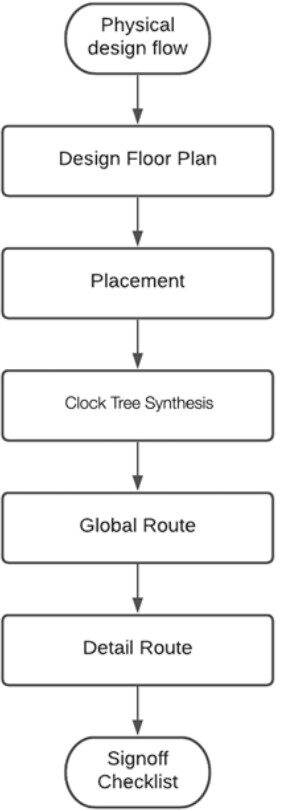
The flow begins with floorplanning, where the die size is determined, macros are positioned, power domains are created, and routing corridors are reserved. This step defines the physical architecture of the chip.
Once the floorplan is finalized, standard cell placement begins. Here, millions of small logic cells are arranged in rows with careful attention to timing and congestion. Placement quality directly influences the complexity of routing and timing closure.
Next comes Clock Tree Synthesis (CTS), one of the most critical steps in PD. The goal is to distribute the clock signal across the design such that all sequential elements receive it with minimal skew and acceptable insertion delay. This ensures synchronous behavior across the chip.
Following CTS, the tool performs routing, where actual metal paths are created to connect every signal. Routing occurs in two phases: global routing, where coarse paths are estimated; and detailed routing, where exact tracks and vias are assigned.
Finally, the design undergoes a series of signoff checks. These include Static Timing Analysis (STA), Design Rule Checks (DRC), Layout vs Schematic (LVS), IR drop estimation, and electromigration analysis. Only after clearing all signoff conditions can the design be exported as a GDSII file for fabrication.
5. Floor planning – The Blueprint of a Successful Chip
Floor planning in Physical design flow is the most influential stage in PPA (Power, Performance, Area) success.
A good floor plan places memory macros close to their controlling logic, keeps analog blocks isolated from switching noise, and ensures that interconnect lengths remain manageable. It also requires establishing power architecture, including power rings and core power grids.
Floor planning sets the stage for the entire PD cycle. A suboptimal floor plan will create congestion hotspots, power integrity challenges, and timing bottlenecks that may require endless iterations to fix later in the flow.
6. Library Characterization and Estimation Models
The Liberty (.lib) files contain detailed timing models and power data for each cell, built through extensive transistor-level simulations.
Every cell is characterized by input transitions, output loads, propagation delays, and power behavior. These data points allow timing and power engines to evaluate full-chip performance accurately.
In early design stages, before routing completes, wire-load models offer rough delay estimates for interconnects. Although approximate, they help guide synthesis and early PD decisions until actual RC (resistance-capacitance) information becomes available from extracted parasitics.
7. The Special Nature of Analog and Mixed-Signal Physical Design
Unlike digital flows that rely heavily on automated EDA tools, analog and mixed-signal (AMS) blocks require manual, transistor-level layout. Designers must carefully place matched devices, minimize parasitic mismatches, shield sensitive nets, and ensure noise isolation.
Custom layout techniques, schematic-driven design, SPICE simulations, and rigorous DRC/LVS checks guarantee the accuracy required for components such as PLLs, data converters, sensors, and RF front ends.
8. EDA Tools – The Workhorses of Physical Design
Physical Design cannot be performed manually on a scale. The chapter highlights that PD tools integrate placement engines, routing algorithms, extraction modules, graphical floor planning interfaces, and signoff-quality verification. They run on high-compute servers because modern SoCs contain billions of transistors.
The chapter also notes an emerging trend: ML/AI-powered EDA tools that learn from past runs and optimize PPA more intelligently. As designs migrate to 7 nm and below, algorithmic intelligence becomes indispensable.
9. The Future of PD – Autonomous and Multi-Dimensional
The physical design trends for advanced chip design are Machine learning–driven timing closure, 3D-IC platforms supporting chiplets, and unified design environments are becoming the future. Designers must adapt to multi-physics and multi-domain workflows.
Physical Design is evolving rapidly, and mastering its flow is essential for engineers entering the semiconductor industry.
Stay Ahead with StarVLSI
If this deep dive into the SoC Physical Design flow inspired you, subscribe to the StarVLSI blog for more industry-driven insights, tutorials, and semiconductor trends.
To stay relevant and accelerate your VLSI career, register for our specialized StarVLSI courses, designed to prepare you for real-world chip design roles and help you contribute confidently to advanced SoC projects.
StarVLSI – Learn. Build. Lead the Future of Silicon.