After floorplanning, placement, and clock tree synthesis, an SoC design reaches one of its most critical and challenging stages—routing. Routing is the process of physically connecting all signal nets, clocks, and power lines while meeting stringent timing, signal integrity, and manufacturability constraints.
In modern SoCs, routing is no longer just about connectivity. It directly impacts performance, power, reliability, and yield, making it a decisive factor in achieving first-pass silicon success.
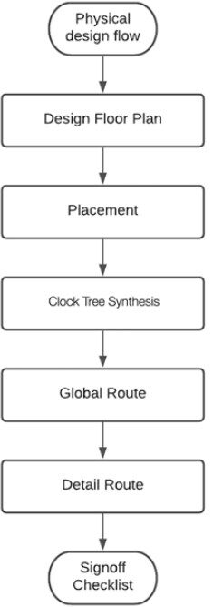
The complete flow diagram describes how a physical design is done.
The flow begins with floorplanning, placement and CTS which were covered in the previous blogs. This blog explores the routing fundamentals, methodologies, algorithms, and challenges in SoC physical design.
Routing in SoC Physical Design
Routing is the process of mapping the logical netlist connections onto physical metal wires and vias while strictly adhering to fabrication rules defined by the foundry. Each net must be connected correctly, efficiently, and reliably without violating spacing, width, or density constraints.
The routing stage must ensure that signal paths meet timing requirements, avoid excessive coupling noise, and remain manufacturable across all process corners. In advanced technology nodes, interconnect delay and parasitic effects often dominate over transistor delay, making routing a critical determinant of overall chip performance.
Preparing the Design for Routing
A design must be carefully prepared before routing begins. Placement and clock tree synthesis need to be stable, power and ground networks must be fully defined, and congestion estimates should indicate that routing resources are sufficient. If these prerequisites are not met, routing can become excessively iterative and may result in poor quality of results.
Design readiness ensures that routing tools can focus on optimization rather than struggling to resolve fundamental structural issues.
Challenges in Signal Routing
Signal routing in SoCs faces multiple challenges due to the scale and complexity of modern designs. High cell density often leads to routing congestion, particularly around macros, memory blocks, and clock distribution regions. Long interconnects introduce delay and degrade timing margins, while closely spaced wires increase the risk of crosstalk and noise coupling.
At advanced nodes, resistance of narrow metal wires increases significantly, and variations in manufacturing processes further complicate routing closure. These challenges demand intelligent, congestion-aware, and timing-driven routing strategies.
Routing Flow in SoC Physical Design
Routing is typically executed in two major phases: global routing and detailed routing.
Global routing provides a high-level plan for how each net will traverse the chip. Instead of defining exact wire geometries, it estimates routing paths and resource usage across routing regions. This phase helps identify congestion hotspots early and guides the detailed router in making efficient decisions.
Detailed routing follows global routing and determines the exact physical implementation of each net. At this stage, precise wire shapes, widths, spacing, and via placements are finalized. Detailed routing must satisfy all design rule checks (DRC) and is computationally intensive due to the sheer number of constraints involved.
Routing Algorithms and Tool Intelligence
Modern electronic design automation (EDA) tools rely on sophisticated routing algorithms to handle large-scale SoC designs. Traditional concepts such as maze routing form the theoretical foundation, but practical routers use heuristic and optimization-based techniques to achieve scalability.
These routers dynamically analyze congestion, timing criticality, and design rules while iteratively refining routes. Nets that violate constraints are often ripped up and rerouted multiple times until an acceptable solution is found.
Timing-Driven Routing
Timing considerations are deeply intertwined with routing decisions. Critical signal paths are prioritized during routing to minimize delay and preserve setup and hold margins. Routing tools may choose higher metal layers with lower resistance, reduce via count, or shorten wire lengths for timing-critical nets.
Without timing-driven routing, a design that meets timing before routing can easily fail after parasitic effects are introduced.
Signal Integrity Considerations
As interconnect spacing decreases, signal integrity becomes a major concern during routing. Crosstalk occurs when signals on adjacent wires interfere with each other due to capacitive or inductive coupling. This interference can cause glitches, delay variation, or even functional failures.
Routing tools mitigate these issues by increasing spacing between sensitive nets, introducing shielding wires, or assigning critical signals to specific routing layers. Antenna effects, which can damage gate oxides during fabrication due to charge accumulation on long wires, are also addressed through routing strategies and protective structures.
Routing for Reliability and Manufacturability
Routing decisions must ensure long-term reliability of the SoC. High current density in narrow wires can lead to electromigration, while voltage drops across power networks can degrade performance. Special routing techniques, such as wider power rails and redundant vias, are employed to ensure robustness.
Manufacturability is equally important. Routing must comply with foundry-specific design rules and density requirements to avoid yield loss. This makes routing a key contributor to design-for-manufacturability (DFM).
Routing and Physical Design Closure
Routing is tightly coupled with static timing analysis, signal integrity checks, and physical verification. It is rarely a one-pass activity. Instead, routing undergoes several optimisation cycles until timing, power, reliability, and DRC requirements are all satisfied.
Successful routing brings the SoC design closer to tape-out readiness, converting abstract functionality into a silicon layout that can be fabricated reliably.
CTS in AI and Large-Scale SoCs
Routing is the stage where SoC design truly becomes real. It bridges the gap between logical intent and physical implementation, balancing connectivity, performance, power, and reliability. As SoC complexity continues to grow, routing remains one of the most demanding and skill-intensive aspects of physical design.
For aspiring and practicing VLSI engineers, a strong understanding of routing principles and challenges is essential for achieving first-time-right silicon.
Acknowledgements:
This blog is conceptually derived from Chapter 5: Routing in SoC Physical Design of the book SoC Physical Design: A Comprehensive Guide, authored by Dr. Veena S. Chakravarthi and Dr. Shivananda R. Koteshwar.
The authors’ extensive industry and academic experience has provided invaluable insights into modern SoC physical design practices. Their work serves as a strong foundational reference for understanding routing methodologies, algorithms, and challenges in contemporary semiconductor design flows.
StarVLSI gratefully acknowledges the authors for their contribution to VLSI education and for advancing practical knowledge in SoC physical design.
Stay Ahead with StarVLSI
To explore more in-depth topics on SoC physical design, routing strategies, and backend VLSI flows, subscribe to the StarVLSI Blog and stay connected with industry-focused learning.
Visit StarVLSI to discover training programs, mentoring initiatives, and career opportunities in semiconductor design.
StarVLSI – Learn. Build. Lead the Future of Silicon.