Best VLSI Training Institutes for Backend Physical Design in Bangalore & Hyderabad
By StarVLSI Editorial Team · March 2025 · 14 min read
Hundreds of ECE graduates search every month for the best VLSI training institutes in Bangalore and Hyderabad — but very few ask the right question: does this institute actually teach Backend Physical Design at industry depth? This guide answers that — and helps you separate genuinely industry-ready PD training from generic VLSI courses that barely scratch the surface.
Why Backend Physical Design Is the Most In-Demand VLSI Specialisation Right Now
Among all VLSI disciplines — RTL Design, DFT, Verification, Analog Layout — Backend Physical Design consistently sees the highest volume of open positions across semiconductor companies in Bangalore and Hyderabad. The reason is straightforward: every chip that gets taped out needs a physical design team, and the flow has grown so complex that companies can no longer afford engineers who learned PD from textbooks alone.
Physical Design engineers are responsible for taking a synthesised netlist and converting it into a manufacturable layout — managing everything from floorplanning and power delivery to timing closure, IR drop, and DRC/LVS signoff. It is one of the most tool-intensive, flow-intensive disciplines in chip design, which is precisely why a VLSI course with genuine hands-on EDA access matters so much.
What a Real Backend Physical Design VLSI Course Must Cover
Before evaluating any VLSI training institute in Bangalore or VLSI training institute in Hyderabad, you need to know exactly what a PD curriculum should contain. Anything less than the following is not preparing you for industry.
If a VLSI course skips even two or three of these stages — or covers them only as theory with no tool labs — it will not prepare you for a Physical Design Engineer interview at any Tier 1 semiconductor company.
How to Evaluate VLSI Training Institutes in Bangalore for PD
Bangalore is home to the largest concentration of semiconductor companies in India — Intel, Qualcomm, NVIDIA, ARM, Synopsys, Cadence, MediaTek, and dozens of fabless design houses. Naturally, it also has the highest number of VLSI training institutes in Bangalore competing for your attention. Here is how to cut through the noise specifically for Backend Physical Design:
Ask for the LinkedIn profile of the Backend PD trainer. They should have at least 5 years of hands-on Physical Design experience at a semiconductor company — not just a teaching background or a general VLSI background.
The institute must have licensed access to Cadence Innovus, Tempus, Voltus, and Pegasus — or Synopsys ICC2 and PrimeTime. If they offer only open-source tools or simulation-only labs, the training is not industry-aligned for Physical Design.
Any credible VLSI training institute in Bangalore should be able to show you a sample floorplan, a timing report, or a DRC summary from a real student project. If they can't — or won't — that tells you everything.
Ask specifically for alumni placed in Physical Design roles — not a general "VLSI placements" figure. Look for company names and verify on LinkedIn. PD placements at Tier 1 companies are the only real proof of training quality.
Backend PD requires individual guidance during tool labs — especially during CTS, timing closure, and DRC debugging. Batches above 30–35 students with a single trainer cannot provide this level of attention. Smaller, focused cohorts consistently produce better-placed engineers.
The Top 10 VLSI Training Institutes in Bangalore: What the Best Ones Have in Common
When you survey the top 10 VLSI training institutes in Bangalore by placement outcomes for Physical Design specifically, a clear pattern emerges. The ones that consistently place engineers at Qualcomm, Intel, MediaTek, and Broadcom all share the same traits: full PD flow coverage (RTL to GDSII), licensed EDA tools, industry-experienced faculty, PDK-based project work, and structured interview preparation. Institutes that shortcut even one of these pillars show noticeably weaker placement records for PD roles specifically.
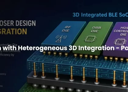
StarVLSI — Backend Physical Design Program
StarVLSI's Backend Physical Design course is built end-to-end around the full Cadence flow — from RTL synthesis in Genus through placement, CTS, and routing in Innovus, timing signoff in Tempus, power integrity in Voltus, and physical verification in Pegasus. Every lab is PDK-based. Faculty are engineers currently working in active PD roles at Tier 1 semiconductor companies. The program runs as a structured offline cohort with small batch sizes, dedicated one-on-one mentoring, and placement preparation embedded throughout — not as an afterthought at the end.
Other established VLSI institutes in Bangalore with a Physical Design track include Maven Silicon, Entuple Technologies, and VLSI Guru — all located in the Marathahalli–Whitefield–Electronic City corridor, close to Bangalore's semiconductor company cluster. Each has strengths worth evaluating, and the criteria above give you a framework to do so objectively.
How to Evaluate VLSI Training Institutes in Hyderabad for PD
Hyderabad's semiconductor footprint has expanded rapidly. Micron Technology's major manufacturing investment, Broadcom's growing design centre, and Samsung Semiconductor's R&D operations have created genuine demand for trained Physical Design engineers in the city. As a result, VLSI training in Hyderabad has grown significantly — but the quality of PD-specific training varies widely.
Students looking at VLSI institutes in Hyderabad for Backend Physical Design should apply the same evaluation criteria as Bangalore. The Hyderabad semiconductor cluster is concentrated around HITEC City, Gachibowli, and Madhapur — so proximity to this corridor matters for networking, guest sessions, and eventual interviews.
- Faculty must have direct PD project experience — HITEC City-based company experience is a strong signal
- Curriculum must cover the full backend flow: synthesis → floorplan → P&R → STA → power → DRC/LVS → GDSII
- EDA tool access must include Cadence Innovus or Synopsys ICC2 with proper licensing
- Projects should use a real industry PDK — not simplified academic examples
- Ask for specific alumni who got placed in PD roles at Micron, Broadcom, or Samsung Hyderabad
- Batch size and mentoring structure should allow for individual guidance during tool labs
Credible VLSI training institutes in Hyderabad with a Physical Design offering include VLSI Expert and Techvolt Solutions. Both operate from the HITEC City corridor and have verifiable placement records worth examining. As with Bangalore, the quality of the individual trainer and the depth of tool lab access are the decisive factors — not the brand name of the institute.
Bangalore vs. Hyderabad: Which City's VLSI Institutes Are Better for PD Training?
| Factor | Bangalore | Hyderabad |
|---|---|---|
| PD-hiring company density | Very high — Qualcomm, Intel, NVIDIA, ARM, MediaTek, Cadence, Synopsys | High and growing — Micron, Broadcom, Samsung Semi, TSMC R&D |
| Number of PD-focused institutes | 8–10 with a genuine PD track | 4–6 with a genuine PD track |
| Faculty access to industry professionals | Highest in India | Strong and improving |
| Interview opportunity proximity | Walk-in drives, frequent campus connects | Growing — especially for Micron and Broadcom |
| Training competitiveness | More options, requires careful evaluation | Fewer but more focused options |
For most students, the decisive factor is not city — it is the individual program's PD curriculum depth, faculty quality, and placement network. The best VLSI training institutes in Bangalore and the best VLSI training institutes in Hyderabad are more similar than different at the top tier. What separates them from mediocre institutes is not geography — it is execution.
Red Flags: When a "VLSI Training Institute" Is Not Worth Your Time
The search volume for VLSI training institutes in Bangalore and VLSI training in Hyderabad has created a market where some institutes prioritise marketing over substance. Watch for these warning signs before you commit:
- PD curriculum described in vague terms like "physical design concepts" with no mention of specific tool flows or PDK-based labs
- Faculty with only academic backgrounds — no active or recent industry project experience in Physical Design
- No licensed Cadence or Synopsys EDA tools — PD training without Innovus, Tempus, or ICC2 is not industry-relevant
- "100% placement" claims with no verifiable alumni list showing PD-specific roles at named companies
- Batch sizes of 50+ students with a single PD instructor — timing closure and DRC debugging require individual guidance
- Curriculum that lumps PD together with Verification, RTL, and DFT into a single generic "VLSI course" — you cannot go deep enough in PD with this structure
- No demo class or trial session offered — credible institutes are confident enough to let you experience the training before committing
- Curriculum not updated to cover advanced nodes (below 28nm) or modern signoff requirements (MCMM STA, low-power flows, advanced DRC)
What Industry Expects from a Fresher Physical Design Engineer
Understanding what VLSI companies in Bangalore and Hyderabad actually interview for gives you a clear benchmark for evaluating any PD training program. Based on interview patterns across semiconductor companies, here is what a fresher Physical Design Engineer is expected to demonstrate on Day 1:
| Interview Area | What Interviewers Test | Covered at Good PD Institutes? |
|---|---|---|
| Floorplanning Concepts | Aspect ratio, macro placement, power grid planning, IO pad placement | ✓ Should be a full lab module |
| Clock Tree Synthesis | Skew budgeting, useful skew, buffer tree structure, CRPR | ✓ Must include tool-based CTS lab |
| Static Timing Analysis | Setup/hold, path tracing, MCMM, ECO flows | ✓ Tempus/PrimeTime lab required |
| Physical Verification | DRC rule types, LVS mismatches, ERC, debugging methodology | ✓ Calibre/Pegasus lab required |
| Low Power Design | Multi-Vt, power gating, UPF basics, voltage domains | Often missing — verify explicitly |
| Tool Scripting (Tcl) | Writing constraints, automating checks, reading reports | Often missing — verify explicitly |
Any VLSI training institute in Bangalore or Hyderabad that skips Low Power Design concepts and Tcl scripting is leaving you underprepared for the interview questions that filter out a significant percentage of PD candidates at Tier 1 companies. Make sure both are part of the curriculum before you enroll.
StarVLSI's Backend Physical Design Program: Built for Industry From Day One
StarVLSI's Backend Physical Design training is structured around a single principle: every hour of training should map directly to something an interviewer at Qualcomm, Intel, or Broadcom will test you on. The program does not offer a diluted overview of all VLSI domains — it goes deep into Physical Design and nothing else.
- Complete Cadence backend flow: Genus (Synthesis) → Innovus (Floorplan, Placement, CTS, Routing) → Tempus (STA) → Voltus (IR/EM) → Pegasus (DRC/LVS)
- All labs use an industry-grade PDK — every student generates real PD deliverables including routed DEF, timing reports, and DRC-clean GDSII
- Low Power Design module: multi-Vt strategies, UPF-based power intent, voltage domain isolation
- Tcl scripting module: constraint writing, report automation, tool flow scripting
- Advanced STA: MCMM setup, ECO flows, timing closure techniques at sub-28nm nodes
- Mock interviews conducted by active industry professionals — not just trainers
- Resume building focused specifically on PD project deliverables that interviewers respond to
- Small cohort structure with dedicated one-on-one lab time for CTS and timing closure guidance
The next Backend Physical Design batch starts 30 March 2025. Batch size is intentionally kept small to preserve the quality of individual mentoring — seats fill quickly each cycle.
Frequently Asked Questions
Ready to Build a Career in Backend Physical Design?
StarVLSI's next Backend Physical Design cohort begins 30 March 2025. Full Cadence flow, PDK-based projects, industry mentors, and dedicated placement support.