SoC physical design has evolved dramatically over the past few decades—from relatively straightforward layout tasks to one of the most complex engineering disciplines in semiconductor development. As technology nodes shrink and system complexity grows, physical design engineers are no longer just implementers of layouts; they are key contributors to system performance, power efficiency, and product success.
Here we highlight how emerging technologies, advanced design methodologies, and evolving skill requirements are shaping the future of SoC physical design
Increasing Complexity in Modern SoCs
Modern SoCs integrate CPUs, GPUs, AI accelerators, high-speed interfaces, memories, and analog components on a single chip. This level of integration places enormous pressure on physical design flows.
Designers must handle billions of transistors, multiple clock and voltage domains, and strict power and thermal constraints. Physical design is no longer isolated—it must align closely with architecture, RTL design, verification, and packaging teams from the earliest stages.
Impact of Advanced Technology Nodes
As technology nodes move into deep nanometer and sub-5nm regimes, physical effects dominate design behavior. Interconnect resistance, parasitic capacitance, variability, and reliability concern significantly affect timing and power.
Design rules have become increasingly restrictive and complex, making layout closure more challenging. At these nodes, physical design decisions directly influence yield and long-term silicon reliability, elevating the importance of backend expertise.
Rise of Power-Driven and Thermal-Aware Design
Power efficiency has become a primary design objective rather than an optimization step. Physical design engineers must now account for dynamic power, leakage, IR drop, and thermal effects throughout the flow.
Thermal-aware placement, robust power grid design, and advanced low-power techniques are becoming standard practice. The future of SoC design demands engineers who can balance performance and power holistically.
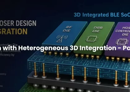
New Design Paradigms: Chiplets and Advanced Packaging
The industry is increasingly adopting chiplet-based architectures and advanced packaging technologies such as 2.5D and 3D integration. These approaches change the scope of physical design beyond a single die.
Physical designers must understand inter-die connectivity, package-level constraints, and signal integrity across chip boundaries. This shift expands the role of physical design into system-level implementation.
Automation, AI, and Tool Evolution
EDA tools are evolving rapidly, incorporating automation and AI-driven optimization techniques. Machine learning is being applied to placement, routing, congestion prediction, and timing closure.
While tools are becoming more powerful, they still require strong engineering judgement. The future physical design engineer must understand both the underlying principles and how to effectively guide advanced tools toward optimal solutions.
Verification and Sign-off Challenges
Sign-off requirements continue to expand, with increasing emphasis on reliability, manufacturability, and variation-aware analysis. Advanced sign-off flows integrate timing, power, signal integrity, and physical verification into unified closure strategies.
Engineers must be comfortable navigating complex sign-off criteria and understanding the trade-offs involved in achieving first-time-right silicon.
Evolving Skill Sets for Physical Design Engineers
The role of a physical design engineer is becoming broader and more interdisciplinary. Beyond tool expertise, engineers must develop strong fundamentals in device physics, interconnect behavior, power integrity, and system-level thinking.
Communication and collaboration skills are also increasingly important, as physical design interacts closely with multiple teams across the product lifecycle.
Preparing for the Future of Physical Design
To stay relevant, physical design engineers must continuously update their skills and adapt to new technologies. Hands-on experience, exposure to real-world sign-off challenges, and a strong conceptual foundation are essential.
Training programs and industry-aligned learning play a critical role in bridging the gap between academic knowledge and production-level design expertise. As technology advances, physical design engineers will play an even more critical role in shaping performance, power efficiency, reliability, and manufacturability of future silicon.
Success in this domain requires not only technical depth but also adaptability, system awareness, and continuous learning. The future of semiconductor innovation depends heavily on the strength of physical design expertise.
Acknowledgement
This blog is conceptually derived from Chapter 10: Future Trends and Challenges in SoC Physical Design of the book SoC Physical Design: A Comprehensive Guide, authored by Dr. Veena S. Chakravarthi and Dr. Shivananda R. Koteshwar.
The authors bring together decades of industry and academic experience to highlight emerging technologies, evolving design methodologies, and the skill transformation required for next-generation SoC physical design engineers. StarVLSI gratefully acknowledges their contribution to advancing VLSI education and shaping future-ready semiconductor professionals.
To prepare for the future of SoC physical design and build industry-ready backend skills,
subscribe to the StarVLSI Blog for expert insights and learning resources.
Visit StarVLSI to explore advanced training programs, hands-on labs, and mentoring designed for the next generation of VLSI engineers.