As semiconductor technology pushes into smaller geometries and higher performance requirements, chip design complexity continues to skyrocket. From smartphones and AI accelerators to IoT and medical devices, every advanced electronic system relies on one crucial stage of the design cycle — Physical Design (PD).
This is where digital logic meets silicon reality — where a high-level hardware description (RTL) becomes an optimized and manufacturable layout (GDSII). Learn how it all begins in our guide on What is RTL Design?
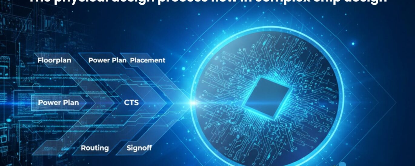
In this guide, we’ll walk through the Physical Design process flow, from floorplanning to tapeout, and highlight the key challenges engineers face when designing complex chips at advanced process nodes like 7nm, 5nm, and 3nm.
What Is Physical Design in VLSI?
Physical Design (PD) is a key stage in the VLSI design flow where a synthesized netlist is converted into a physical layout ready for fabrication. It involves multiple iterative steps that balance timing, power, area, and signal integrity using advanced EDA tools. For a detailed industry overview, check out Synopsys Physical Design Solutions.
The input to Physical Design includes:
-
Synthesized netlist
-
Timing constraints (SDC files)
-
Power intent files (UPF/CPF)
-
Foundry technology files (LEF, DEF, LIB)
-
Floorplan guidelines and design targets
Once these are ready, the chip design process moves through several critical stages.
The Physical Design Flow: Step-by-Step
1. Floorplanning
Floorplanning defines the blueprint of the chip — determining the size, shape, and placement of macros, memory blocks, and I/O pins. A strong floorplan reduces routing congestion, improves timing, and enables efficient power delivery.
🧩 Tip: A poor floorplan can make timing closure nearly impossible later.
2. Power Planning
Next comes power network design — building power rings, straps, and grids to distribute voltage reliably across the chip. Engineers must manage IR drop, electromigration, and multi-voltage domains.
💡 Techniques like power gating and clock gating help reduce leakage and dynamic power.
3. Placement
In placement, standard cells are positioned within the floorplan to meet timing and congestion constraints. Modern tools use timing-driven placement and iterative optimization to balance wirelength and performance.
⚙️ A good placement reduces delay, avoids hotspots, and sets up smooth routing.
4. Clock Tree Synthesis (CTS)
The clock is the heartbeat of the chip. During Clock Tree Synthesis, designers distribute the clock signal uniformly across all sequential elements, minimizing skew and insertion delay.
⏱ Optimizing the clock network is critical because it consumes significant dynamic power.
5. Routing
Routing connects all the placed cells with metal wires according to design rules. It consists of:
Global routing: planning wire paths
Detailed routing: assigning exact metal layers and tracks
Modern routers handle crosstalk, antenna effects, and DRC violations automatically, but manual tuning is often needed at advanced nodes.
6. Signoff and Tapeout
Before sending the design to the foundry, it undergoes signoff checks:
Static Timing Analysis (STA)
Power integrity checks (IR drop, EM)
Physical verification (DRC/LVS)
Once all checks pass, the final layout is converted into GDSII format and sent for fabrication — a milestone known as tapeout.
Challenges in Modern Physical Design
Designing chips at advanced technology nodes (7nm, 5nm, 3nm) introduces several challenges:
Multi-mode, multi-corner (MMMC) timing closure
Dense routing and power distribution networks
Complex DRC and lithography rules
Thermal and IR drop constraints
High tool runtime and compute resource demands
Modern PD engineers rely heavily on AI-assisted EDA tools, automation scripts, and machine learning models to optimize Power, Performance, and Area (PPA) efficiently.
Conclusion
Physical Design is not just a step in chip development — it’s the heart of silicon realization.
From RTL to GDSII, every stage requires precision, expertise, and cutting-edge EDA tools to meet aggressive design targets.
In upcoming posts, we’ll dive deeper into each phase — sharing hands-on strategies, real-world examples, and best practices for engineers and enthusiasts in the VLSI industry.
👉 Follow the starVLSI Blog for deep dives into floorplanning, CTS, routing optimization, and signoff automation.