
The semiconductor industry is entering an exciting and demanding phase, advanced nodes, 3D integration, AI-assisted design, and global chip initiatives are reshaping the skill map for VLSI designers. While real-world project experience remains the ultimate credential, structured certifications now play a vital role in establishing credibility, building tool proficiency, and showcasing readiness for complex SoC and chip design challenges.
This blog highlights the most relevant certifications and learning domains that aspiring VLSI and EDA professionals should pursue in 2026 to stay competitive and job-ready.
Certifications Matter but They’re Not Everything
VLSI design projects today span multiple disciplines, from RTL development and verification to layout, sign-off, and test automation. Each domain uses highly specialized EDA tools such as Cadence Virtuoso, Synopsys Design Compiler, Siemens Calibre, or Xcelium. Recruiters and project leads look for engineers who can not only code and simulate but also understand tool flows, timing closure, and manufacturability constraints.
Certifications offer:
- A structured path to learn industry-standard tools and flows
• A recognizable credential that demonstrates formal training
• A bridge for fresh graduates to enter professional design teams
However, industry veterans unanimously agree on one thing, certifications support, but never replace, hands-on design experience. A designer’s true value comes from debugging real projects, closing timing, and seeing silicon results.
The Evolving Skill Map for 2026
As semiconductor ecosystems evolve, new competencies are emerging across design, verification, and automation. Here are the key certification domains every aspiring VLSI designer should explore.
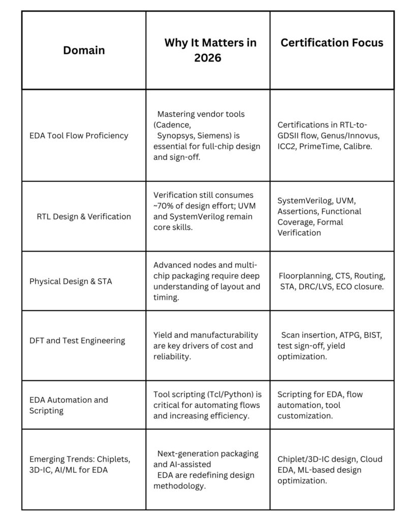
Below are the most valuable certification tracks categorized by career stage.
Early-Career for aspiring Students & Fresh Graduates
These certifications help build a strong foundation across design, verification, and layout flows.
- Fundamentals of VLSI Design and EDA Tools
– Offered by: NIELIT, VLSI Society of India, Cadence Academic Network
– Covers: RTL-to-GDS flow, Virtuoso, Genus, Innovus, Tempus
– Ideal for: Beginners who want structured exposure to EDA tool environments
2. Vendor Entry-Level Badges (Synopsys / Cadence / Siemens)
– E.g., Synopsys Purple Certification
– Focus: Basic synthesis, simulation, or verification tool usage
3. Verification Basics – SystemVerilog/UVM Certification
– Focus: Testbench design, coverage, assertions
4. Scripting for VLSI Automation (Tcl/Python)
– Focus: Automating tool flows, regression environments, and design checks
Mid-Level for Design Engineers, Project Leads
These certifications deepen expertise and improve domain specialization.
- Physical Design & Sign-Off Expert Certification
– Covers: Floorplanning, CTS, routing, STA, and sign-off with Innovus/ICC2
– Useful for: Engineers aiming for PD or STA specialization2. Advanced Verification Methodology (UVM/Formal)
– Focus: Advanced testbench architecture, low-power verification, coverage closure3. DFT and Test Engineering Certification
– Covers: ATPG, scan insertion, BIST, test synthesis, yield improvement4. Analog/Mixed-Signal & Low-Power Design
– Covers: Layout methodologies, power domains, verification with UPF/CPF5. Custom Flow and Automation Expert Track
– Focus: Building custom scripts and automated verification frameworks using Python/Tcl
Future-Ready for Emerging & Cross-Domain Skills
To remain ahead of the curve, designers should explore certifications that prepare them for the next decade of semiconductor design.
- 3D-IC and Chiplet Design Certification – Learn design partitioning, packaging integration, and interconnect modeling
• AI/ML for EDA Applications – Explore how ML assists PPA optimization, verification, and anomaly detection
• Cloud EDA and Collaborative Design Environments – Understand how distributed cloud environments are transforming tape-out processes
Practical Advice for Aspiring Designers
- Start with fundamentals, then specialize: choose one core domain (Design, Verification, PD, DFT, or AMS).
2. Pick certifications that include hands-on projects, not just multiple-choice exams.
3. Get familiar with at least one full tool chain (e.g., RTL → synthesis → STA → layout).
4. Document your certification and project outcomes, maintain a digital portfolio or GitHub-style showcase.
5. Stay updated. Tool versions and methodologies evolve rapidly. Renew or update certifications periodically.
The Real Takeaway
In 2026, the best VLSI designers will not just be tool experts, they’ll be problem-solvers who understand the full chip lifecycle, from architecture to manufacturing. Certifications are valuable stepping stones that help you gain credibility, structured learning, and exposure to EDA ecosystems. But your true expertise will come from solving real problems, debugging real designs, and delivering real silicon.
If you are serious about a career in semiconductor design, combine certifications, continuous learning, and project experience to design the future of intelligent chips.
Author’s Note:
This blog is part of LeadSOC’s continuing effort to guide and mentor young engineers in the semiconductor ecosystem, empowering them with the skills, mindset, and certifications needed for next-generation VLSI design excellence.